The Role of Magnetizing and Leakage Inductance in
advertisement
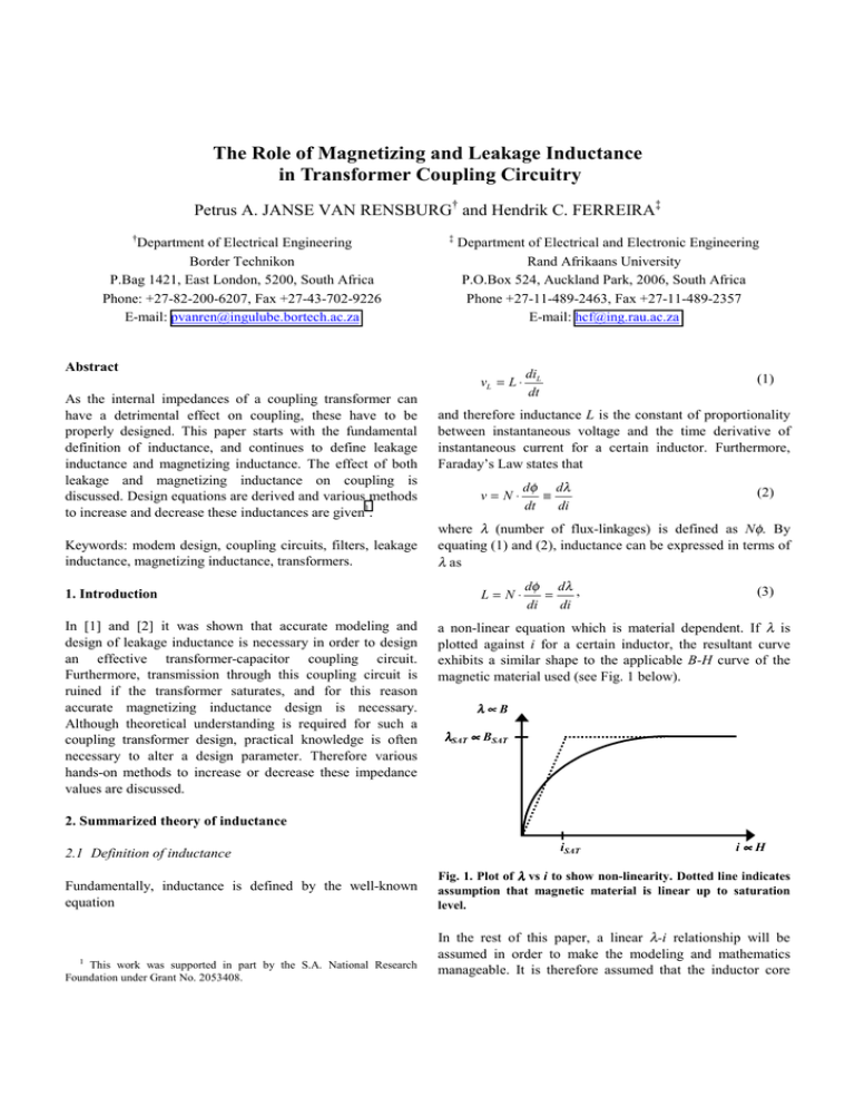
The Role of Magnetizing and Leakage Inductance in Transformer Coupling Circuitry Petrus A. JANSE VAN RENSBURG† and Hendrik C. FERREIRA‡ † Department of Electrical Engineering Border Technikon P.Bag 1421, East London, 5200, South Africa Phone: +27-82-200-6207, Fax +27-43-702-9226 E-mail: pvanren@ingulube.bortech.ac.za ‡ Department of Electrical and Electronic Engineering Rand Afrikaans University P.O.Box 524, Auckland Park, 2006, South Africa Phone +27-11-489-2463, Fax +27-11-489-2357 E-mail: hcf@ing.rau.ac.za Abstract vL = L ⋅ As the internal impedances of a coupling transformer can have a detrimental effect on coupling, these have to be properly designed. This paper starts with the fundamental definition of inductance, and continues to define leakage inductance and magnetizing inductance. The effect of both leakage and magnetizing inductance on coupling is discussed. Design equations are derived and various methods to increase and decrease these inductances are given1. Keywords: modem design, coupling circuits, filters, leakage inductance, magnetizing inductance, transformers. 1. Introduction In [1] and [2] it was shown that accurate modeling and design of leakage inductance is necessary in order to design an effective transformer-capacitor coupling circuit. Furthermore, transmission through this coupling circuit is ruined if the transformer saturates, and for this reason accurate magnetizing inductance design is necessary. Although theoretical understanding is required for such a coupling transformer design, practical knowledge is often necessary to alter a design parameter. Therefore various hands-on methods to increase or decrease these impedance values are discussed. diL dt (1) and therefore inductance L is the constant of proportionality between instantaneous voltage and the time derivative of instantaneous current for a certain inductor. Furthermore, Faraday’s Law states that v= N⋅ dφ dλ ≡ dt di (2) where λ (number of flux-linkages) is defined as Nφ. By equating (1) and (2), inductance can be expressed in terms of λ as L= N⋅ dφ dλ , = di di (3) a non-linear equation which is material dependent. If λ is plotted against i for a certain inductor, the resultant curve exhibits a similar shape to the applicable B-H curve of the magnetic material used (see Fig. 1 below). λ∝B λSAT ∝ BSAT 2. Summarized theory of inductance 2.1 Definition of inductance Fundamentally, inductance is defined by the well-known equation 1 This work was supported in part by the S.A. National Research Foundation under Grant No. 2053408. iSAT i∝H Fig. 1. Plot of λ vs i to show non-linearity. Dotted line indicates assumption that magnetic material is linear up to saturation level. In the rest of this paper, a linear λ-i relationship will be assumed in order to make the modeling and mathematics manageable. It is therefore assumed that the inductor core has a constant µR. (This assumption is accurate only for aircore inductors or cored inductors where excitation is minimal.) Based on this assumption, inductance can now be written as L= N⋅ φ λ, = i i (4) the ratio between total flux-linkage and the current caused by said flux-linkage. In a transformer core, two main flux paths exist, and the associated fluxes are called mutual (or magnetizing) flux and leakage flux. These two flux components are responsible for a transformer’s magnetizing and leakage inductance respectively. For an inductor though, the magnetizing and leakage flux components add to make up the total inductance. Refer to Fig. 2. φM1 φN2 N1 i2 N2 LL = LL1 + LL 2 = N1 ⋅ φL1 φ + N1 ⋅ L 2 i1 i1 (6) Assuming negligible losses and a linear λ-i relationship, the voltages across the primary and secondary windings can be obtained through Faraday’s Law (2): v1 = LL1 di di1 N di + LM 1 − 2 ⋅ 2 dt dt N1 dt (7) di di2 N 2 N di + LM 1 − 2 ⋅ 2 dt N1 dt N1 dt (8) These two equations, with resistors added in order to model losses, give rise to the widely used transformer equivalent circuit shown in Fig. 3 below. For an ideal transformer, the series components need to be negligibly small, whereas the parallel components need to exhibit very large values. RN1 primary core (5) where φM = φM 1 − φM 2 represents the resultant mutual or magnetizing flux. Similarly, the resultant leakage inductance LL can be written as v2 = − LL2 φM2 φL2 φN1 i1 φM i1 where LL1 and LL2 are the primary and secondary leakage inductances respectively. 2.2 Inductance in transformers φL1 LM = N1 ⋅ LL1 LL2 RN2 secondary MMF N1i1 ≈ N2i2 RC LM Ideal core window Fig. 2. Simplified representation of a transformer’s flux paths and MMF distribution across the core window. In Fig. 2., φN1 represents the total flux induced by MMF N1i1. A certain component of φN1 ‘leaks’ back to the bottom leg of the core and is labeled φL1. This primary leakage flux φL1 therefore does not couple with the secondary winding N2. The remaining (mutual) primary flux φM1 however does couple with N2 and induces MMF φN2 in winding N2. Similarly, only φM2, the magnetizing (mutual) portion of φN2 couples with N1, whereas the uncoupled flux φL2 leaks back through the core window. Using (4), the magnetizing inductance LM of a transformer can now be written as Fig. 3. General transformer equivalent circuit, assuming linear core material, losses modeled with resistors. The secondary leakage inductance can be referred to the primary side, but this causes inaccuracies as the magnetizing current does not flow through LL2. For a large magnetizing inductance though, the secondary leakage inductance may be safely referred to the primary side using 2 N LL 2 (referred ) = 1 ⋅ LL 2 N2 3. Leakage inductance considerations (9) As graphically depicted in Fig. 4 the MMF in volume v1 can be written as 3.1 Influence on filtering The leakage inductance of a coupling transformer forms a series-resonant band-pass filter with the external (series) coupling capacitor. For frequencies close to resonance, the effect of the magnetizing inductance is negligible. See section 4 as well as [1] or [2]. 3.2 Calculation of leakage inductance An alternative approach to calculate inductance, is to use two energy equations, namely the energy stored in an inductor (10) as well as the energy stored in a certain threedimensional space through volume-integration of the B-H product (11): W= 2 Li 2 x N1i1 ⋅ a w 0< x < a. (14) Take note that w, the width of a planar winding, represents the effective magnetic path-length of the leakage flux. It is now also assumed that the winding structure, viewed from the top, has a cylindrical shape with average turn-length T in order that dv = A⋅dx = Tw⋅dx. It follows that 2 a µ 0 x N1i1 ⋅ ⋅ ⋅ Tw ⋅ dx a w 0 2 (15) W1 = ∫ 2 a ⇒ W = µ 0 ⋅ N 1i1 ⋅ Tw ⋅ x 2 ⋅ dx 1 ∫ (16) 0 2 (11) By equating (10) and (11), and solving for L, inductance can be expressed as µ 0µ r 2 ∫ H dv . i2 v ⇒ W = µ 0 ⋅ N1i1 ⋅ Tw ⋅ 1 ⋅ a 3 1 2 aw 3 (17) ⇒ W1 = µ 0 aT ⋅ (N1i1 )2 6w (18) Similarly, it can be shown that the leakage energy W2 stored in winding N2 is (12) As an example, the leakage inductance of the following planar transformer in Fig. 4 will be calculated. This transformer has separately wound primary and secondary windings (no interleaving). Also see [3] for a different winding configuration. W2 = µ 0 bT 2 ⋅ ( N1i1 ) 6w (19) as N1i1 ≈ N2i2. Furthermore, the energy stored in volume v3 can be calculated by c secondary winding N2 for 2 aw (10) µ µ 1 W = ∫ BHdv = 0 r ∫ H 2 dv 2v 2 v L= H= 2 µ 0 N1i1 ⋅ ⋅ Tw ⋅ dx w 0 2 W3 = ∫ w X H= b as N1i1 for volume v . Therefore 3 w (20) (21) c a N1i1≈ N2i2 primary winding N1 core Fig. 4. Cross-section through a planar transformer and MMF distribution across window. Assuming that µR = 1 for volumes v1 , v2 , and v3 (volumes taken up by windings N1, N2, and isolation between windings respectively) the leakage inductance can be calculated. The total ‘leakage’ energy stored in volume v1, is given by W1 = ∫ dW1 v1 where dW1 = µ 0 H 2 ⋅ dv1 . 2 (13) W3 = µ 0 cT 2 ⋅ ( N1i1 ) . 2w (22) The total ‘leakage’ energy stored in the transformer can be obtained by adding the individual energy components, and therefore the total energy stored in the ‘leakage inductance’ LL of the transformer is given by WL = W1 + W2 + W3 = 1 LLi 2 2 (23) From (18), (19), (22) and (23) it follows that LL = µ 0 N12T ⋅ ⋅ (a + b + 3c ) 3 w [H] (24) where µ0 = 4πx10-7 is the permeability of free space and N1 the number of turns on the primary winding. T represents the average turn-length whereas w denotes core window width. As shown in Fig. 4, symbols a, b and c represent the thickness of the primary, secondary and insulation layers respectively. For high-frequency applications, the leakage inductance has to resonate with the series coupling capacitor at the carrier frequency. This implies that smaller reactive component values are required. Although it would be the easiest and most economical to reduce the coupling capacitance value, the leakage inductance may have to be reduced in certain cases. Some general guidelines are given below: 3.3 Enlarging leakage inductance • If a transformer’s leakage inductance is to be utilized as a filter inductor (instead of using an external, discrete inductor) its value often has to be increased. A few techniques will be discussed below: • Increase the insulation thickness c between the primary and secondary layers – refer to (24). • Increase the number of turns N1 of the primary (and secondary to keep winding ratio the same). See (24). • Insert ferrite (or other material) with permeability µR between primary and secondary windings to drastically boost the leakage flux. Equation (24) then becomes 2 µ N T LL = 0 ⋅ 1 ⋅ (a + b + 3µ R c) 3 w • [H]. (25) Allow the external winding to protrude out of the core. See Fig. 5 below. If the original leakage inductance of the transformer without the protruding loop is negligible, the leakage inductance with protruding loop is given by an empirical equation [4] 2 LL = N1 R 2 230 R + 250 H [µH] (26) where R and H represent the radius and height of the protruding loop respectively. • • Choose an appropriate core type that encloses the windings to minimize external leakage. Minimize thickness of insulating layer between windings. Interleave layers of primary and secondary windings in order to lower the effective MMF. Using the method described in section 3.2, it can be proven that the theoretical leakage inductance of an interleaved transformer (where the primary winding is divided into q layers and secondary winding is divided into q+1 layers) is given by LL = µ 0 N12T ⋅ ⋅ (a + b + 6c ) 6q w 3.4 Reducing leakage inductance (27) Comparing (25) with (24) it is evident that leakage inductance can be reduced by almost 75% by merely dividing the primary winding into q = 2 layers and the secondary winding into three layers. 4. Magnetizing inductance considerations 4.1 Influence on saturation and filtering As the total flux density in a coupling transformer core is made up of the communication waveform’s flux density superimposed on the filtered power waveform’s flux density, the influence of both have to be considered in order to prevent saturation. The influence of the filtered power waveform on core saturation can be gauged by its v/f factor, also called the volt-time product. Equation (28) refers to Fig. 6(a) and summarizes the super-imposing influence of the filtered power waveform (subscript P) and the referred communication / modem waveform (subscript M) on the total flux density (subscript T), and is valid for sinusoidal waveforms only. BT = BP + BM = Fig. 5. Cross-section through transformer (top view) to indicate winding protruding from core. External loop has a radius R. [H] 1 2πAN V ' V' ⋅ P + M fM fP (28) The ratio of the filtered power waveform’s v/f value to the communication waveform’s v/f value will determine how the two waveforms share (or exceed) the total flux density, as core cross-sectional area (A) and number of primary turns (N) are fixed for a certain design. Take note that in Fig. 6(a) and equation (28) the voltage V’P refers to the peak filtered power voltage, whereas V’M refers to the peak referred communication voltage. Furthermore, the minimum value of fM has to be used in order to calculate the maximum flux density. At a first glance, it seems as if this band-pass coupling circuit designed in [2], would only be able to filter the power waveform by a maximum of 60dB, as only three decades is available for filtering, and the roll-off slope is -20dB/decade. However, it must be emphasized that the model in [2] is only valid for frequencies close to the resonant point. A more comprehensive model of the coupling circuit that includes the magnetizing inductance, is shown in Fig. 6(a). The voltage transfer function of this circuit (in the receiving direction) is expressed by 2 V 'P s RCLM = 3 2 VP s CLM LL + s RC ( LM + LL ) + sLM + R (29) where R represents the referred modem impedance. From (29) it is clear that the power-line impedance has no influence on the voltage transfer function in the receiving direction. The amplitude response of (29) was simulated and is shown in Fig. 6(b). As can be seen in Fig. 6(b), the simulated amplitude response of the coupling circuit under consideration correlates well with the simple band-pass model of [2] for frequencies above 1.6kHz, but a roll-off slope of –40dB/decade is evident below 1.6kHz. This is due to the influence of the parallel magnetizing inductance at lower frequencies. At 1.6kHz, the reactance of this coupling transformer’s 100µH magnetizing impedance nearly equals the 1Ω (referred) load resistor, and at frequencies below 1.6kHz, its reactance dominates the parallel branch (LM||R), attenuating these frequencies more than for a pure resistor. LL V’P + V’M (superimposed) ZP LM R’M ≡R (a) 20 20log10[V’P/VP] (dB) As an example, the coupling circuit designed in [2] will be discussed. This coupling circuit was designed to transmit and receive any 122dBµV or 1.26VPEAK CENELEC B, C, or D signal (95kHz-148.5kHz) to and from a 50Hz, 220VRMS, 1Ω power line. Thus the received communication waveform will have a maximum v/f factor of only 1.26V / 95kHz = 13µV/Hz, yielding a flux density of BM ≈ 9mT for the chosen core set. For the filtered power waveform to have a v/f figure (and flux density contribution) of say twice this value, it needs to be filtered to a voltage of only 1.3mVPEAK or by 107.6dB. Alternatively, a power waveform attenuation level of –100dB would represent 62.2µV/Hz (BP ≈ 43mT) whereas –90dB would represent 196.7µV/Hz (BP ≈ 136.2mT), all still within acceptable limits as BSAT = 400mT for this ferrite core. C VP -10 -40 -70 -100 16 160 1.6k 16k 160k Frequency (Hz) 1.6M 16M (b) Fig. 6. (a) More comprehensive model for the coupling circuit designed in [2] and (b) simulated amplitude response for the coupling circuit designed in [2]. Here the reference level is 0dB as the 1:7 transformer winding ratio was not included in the simulation. It is not necessary to simulate above circuit for every design, as the magnitude of the filtered power waveform voltage for a certain frequency (voltage across the magnetizing inductance) can be calculated using the voltage divider rule: V 'P = X LM X R X C + X LL + ( X LM X R ) ⋅ VP (30) Subscripts LL and LM refer to leakage and magnetizing inductance respectively, whereas subscript R refers to the modem impedance referred to the power-line side. Once V’P is known, its contribution to the flux density can be calculated with (28). The simulated amplitude response (Fig 6(b)) of the coupling circuit designed in [2] was verified practically and a measurement is shown in Fig. 7. In Fig. 7 the general trend of Fig. 6(b) can be seen, although low-frequency values are not as accurate because of a limited bandwidth when scanning a wide frequency range. The coupling circuit deviates from theoretical values for low frequencies. This is partly due to the limited power output of the measuring 20log10[VM/VP] (dB) instrument - the transformer core cannot be driven deeply into saturation. negligible. Leakage inductance can be subtracted from L to obtain more accurate answers for LM. +15 4.3 Enlarging/Reducing magnetizing inductance -15 From equation (33) it is clear that magnetizing inductance can be increased by either increasing µR, increasing A or decreasing l (using a different transformer core), or alternatively increasing N (thinner conductors or bigger core). It must be mentioned that µR is also dependent on the air gap if a core set is used. In this case µR can be boosted by decreasing the air-gap, or even clamping the core set together. -45 -75 -105 -135 10 100 1k 10k 100k Frequency (Hz) 1M 10M Fig. 7. Measured amplitude response of the coupling circuit designed in [2] The cursor was positioned at ≈ 50Hz and measured –83dB (+17dB reference level). From the cursor measurement in Fig. 7 it is evident that for the specific coupling circuit designed in [2], a total attenuation of 100dB is attainable. Thus the power waveform is expected to occupy 43mT of flux density whilst the communication waveform is predicted to utilize 9mT. The sum of these two figures, 52mT, will be the total flux density in the coupling transformer’s core. This value will be the same, regardless of whether the coupling circuit is used to receive data or transmit data: although the voltages on the modem side is seven-fold those on the power line side, the number of turns is also seven-fold and thus cancels the influence of former. 4.2 Calculation of magnetizing inductance It was shown in section 2 that φ L= N⋅ i where ℑ Ni . φ= = ℜ ℜ le µAe (31) (32) where µ represents permeability, le is the effective flux path length and Ae is the effective core cross-sectional area. From (31) and (32) follows that total inductance L = LM + LL = µ0 µ R ⋅ N 2 Ae . le 5. Conclusion In order to design an effective coupling circuit, the internal impedances have to be designed properly, as they can have a detrimental effect on coupling by either (i) filtering the communication signal or (ii) allowing the power waveform to saturate the coupling transformer. Therefore the fundamental definition of inductance, as well as leakage inductance and magnetizing inductance were discussed. Design equations were derived and various practical methods to increase and decrease these inductances were discussed. References Furthermore reluctance ℜ is defined by ℜ= Conversely, magnetizing inductance can be decreased by inserting an air-gap between certain legs of a core. This technique of fine-tuning the air-gap for a certain magnetizing inductance is widely used. Take note that the air-gap doesn’t alter BSAT but only lowers µe to skew the B-H curve [5]. Although BSAT stays the same, a smaller magnetizing inductance would help to filter low frequencies more effectively, as the –40dB/decade slope starts at a higher frequency. Refer to Fig. 6(b) and Fig. 7. (33) Equation (33) gives reasonably accurate values for magnetizing inductance as leakage inductance LL is typically [1] P. A. Janse van Rensburg, H. C. Ferreira, “Coupling circuitry: understanding the functions of different components,” Proc. 7th Int. Symp. Power-Line Comm., 2003, pp. 204-209. [2] P. A. Janse van Rensburg, H. C. Ferreira, “Step-by-step design of a coupling circuit with bi-directional transmission capabilities,” Submitted for 8th Int. Symp. Power-Line Comm., 2004. [3] A. S. Langsdorf, Theory of Alternating-Current Machinery, 2nd ed., New York: McGraw-Hill, 1955, pp. 43-49. [4] P. C. Theron and J. A. Ferreira, “The zero voltage switching partial series resonant converter,” IEEE Transactions on Industry Applications, vol. 31, no. 4, pp. 879-886, July/Aug. 1995. [5] J. G. Kassakian, M. F. Schlecht, G. C. Verghese, Principles of Power Electronics, Reading, Massachusetts: Addison-Wesley, 1991, p. 572.
