University of California at Berkeley College of Engineering
advertisement
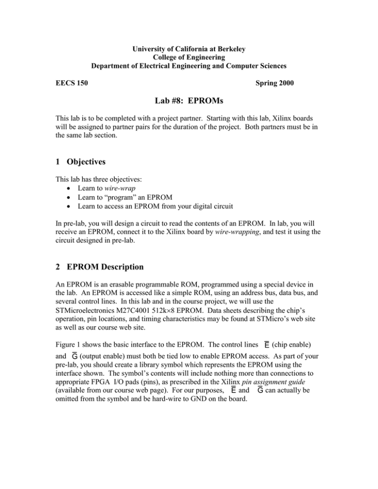
University of California at Berkeley College of Engineering Department of Electrical Engineering and Computer Sciences EECS 150 Spring 2000 Lab #8: EPROMs This lab is to be completed with a project partner. Starting with this lab, Xilinx boards will be assigned to partner pairs for the duration of the project. Both partners must be in the same lab section. 1 Objectives This lab has three objectives: Learn to wire-wrap Learn to “program” an EPROM Learn to access an EPROM from your digital circuit In pre-lab, you will design a circuit to read the contents of an EPROM. In lab, you will receive an EPROM, connect it to the Xilinx board by wire-wrapping, and test it using the circuit designed in pre-lab. 2 EPROM Description An EPROM is an erasable programmable ROM, programmed using a special device in the lab. An EPROM is accessed like a simple ROM, using an address bus, data bus, and several control lines. In this lab and in the course project, we will use the STMicroelectronics M27C4001 512k8 EPROM. Data sheets describing the chip’s operation, pin locations, and timing characteristics may be found at STMicro’s web site as well as our course web site. Figure 1 shows the basic interface to the EPROM. The control lines E (chip enable) and G (output enable) must both be tied low to enable EPROM access. As part of your pre-lab, you should create a library symbol which represents the EPROM using the interface shown. The symbol’s contents will include nothing more than connections to appropriate FPGA I/O pads (pins), as prescribed in the Xilinx pin assignment guide (available from our course web page). For our purposes, E and G can actually be omitted from the symbol and be hard-wire to GND on the board. Chip Enable Output Enable Address E EPROM 512K8 G A[18:0] D[7:0] Data Figure 1: EPROM interface 3 EPROM Test Circuit We have devised an EPROM test scheme based on pointer chasing. The test is designed to fail if you have incorrectly wired any of the address or data signals. On any error, pointer chasing will converge at address $FFFF. On success, it will converge at some other mystery address. Because our 512K8 EPROM uses 8-bit data words, we will store 16-bit pointers in two separate data bytes. We will use a little-endian representation of pointers, where the least-significant byte resides at an address immediately preceding that of the mostsignificant byte. The EPROM actually uses 19-bit addresses, but the test assumes that the top 3 bits are always to 0. The EPROM data file (which we will provide) contains a 16bit pointer at byte locations 0 and 1. This pointer points to (i.e. is the address of) a subsequent pointer, which points to yet another pointer, etc. The final pointer points to itself. You will design and enter a circuit to perform the pointer chasing described above. Figure 2 presents a possible implementation. You should study it carefully. The design stores each pointer in two registers MAR0 and MAR1 (“memory address registers”) representing the low-order and high-order bytes, respectively. A pointer is fetched into these registers in two cycles – a first cycle to fetch the low-order byte into MAR0 (via MDR), and a second cycle to fetch the high-order byte into MAR1. The purpose of MDR (“memory data register”) is to delay the loading of MAR0 for 1 cycle, so that both bytes of a pointer are loaded into MAR0 and MAR1 simultaneously. The controller is a simple, 2-state FSM which alternates state each cycle. The output of the state flip-flop directly controls the loading of registers. Notice that the low bit of the memory address comes from that state flip-flop (not MAR0). A global reset signal is used to initialize the state and all registers. That signal should come from the reset push-button (SW-1, connected to pin 56 when DIP switch SW2-7 is open). Clock the circuit using a 8MHz clock signal. This frequency can be generated from the 16MHz crystal oscillator on pin 13 using a clock divider similar to the one used in the UART lab (lab #7). The frequency 8MHz represents a cycle time of 125ns, slightly longer than the EPROM data access delay of 100ns. To 7-segment LEDs CE RESET MDR CE MAR1 RESET D Q CE MAR0 RESET 8 8 d7..d0 Controller a15..a8 7 a7..a1 a0 Figure 2: EPROM test circuit 4 Wire Wrapping Wire wrapping is the method you will use to make electrical connections on the Xilinx board. It is more reliable and neater than using jumper wires. It involves wrapping the ends of a wire around header pins using a small tool. Wire wrapping will be demonstrated in the lab lecture. CS150 Top Ten Wire Wrap Hints 10. 9. 8. 7. 6. 5. 4. 3. 2. 1. Use wrap IDs Plan your wire routing before beginning to wrap When possible, run wires around chips, not through the middle Use colors to code signal groups Do not push down or pull up on the tool as you turn it Wrap some insulation around the bottom of the pin Keep wires flat and tight Do not be afraid to unwrap and do it over Watch out for little pieces of broken wire Be neat! In the lab, we will provide sheets of wrap IDs for the M27C4001 EPROM. Wrap IDs are a labeling of pin names that may be pasted onto a Xilinx board as an aid for wiring. Cut out a rectangular area of paper containing the IDs and carefully push it onto the pins opposite where the EPROM is to be socketted. Note that the wrap IDs represent a mirror-image of the EPROM’s pinout. Wire wrap the EPROM’s designated pins to the FPGA’s pins as prescribed in the Xilinx pin assignment guide (available on our course web page). As always, be very careful not to damage your board with static charge. Periodically ground yourself by touching a large metal object (or other conducting object, e.g. the anti-static mat used as a work pad). When wiring the EPROM, make sure that its programming voltage line Vpp is tied to GND to disable overwriting of memory contents. Do not forget to tie the enable lines (E’, G’) to GND. 5 Programming the EPROM You will use the Advin Systems’ Pilot-U40 EPROM programmer to load the EPROM with TA-provided content. The programmer resembles a textbook-size, black box and is available at several workstations in the lab. 5.1 Launching the programmer software Open the Advin directory (C:\ADVIN, also via shortcut on the NT desktop). Launch the SPEPROM.EXE program. This is a menu-driven, text-mode program. You can select among menu options using the and arrow keys, choose a menu option using or Enter, and exit from a menu using or ESC. 5.2 Software settings Select the proper device using the menu selection: ConfigDeviceSTM27C4001, or alternatively: ConfigDeviceGeneric27C040. When using the Generic driver, a listing of compatible devices should appear, including our device: 27C4001. WARNING: Failure to configure the programmer software for the correct device may result in permanent damage to the EPROM. Set the software correctly, and verify that the device number M27C4001 appears on the EPROM package. Load the TA-provided EPROM contents from file, using the menu selections: FileNameU:WVLIB\CS150\LAB8\EPROM.BIT (alternatively, use: C:\CS150\LAB8\EPROM.BIT) and: FileLoad. You will need to exit several menu levels first. 5.3 Programming the EPROM Place the EPROM in the programmer socket a) Lift up the lever arm. b) Place the M27C4001 into the socket, oriented as in the diagram on the programmer. The chip should be flush with the top of the socket, with the notch pointing up. c) Lower the lever arm to lock the chip in place. Verify that the EPROM is empty using a blank check: PROMBlank. If the EPROM is not blank, you must erase it before programming (see below). Download the TA-provided content into the EPROM: PROMProgram. The programmer software will draw smiley faces to indicate progress. Remove the EPROM from the programmer. It is now ready for testing with your circuit. 5.4 Erasing the EPROM The EPROM can be erased by exposing it to strong ultraviolet light (UV). Place the EPROM into the eraser, with its small transparent window facing up (when erasing, a fluorescent UV bulb will illuminate the chip from above). Erasing takes about 15-20 minutes. Set the timer accordingly. Multiple chips may be erased in tandem. Avoid looking at the UV light. It may result in eye damage. 6 Lab Assignment For pre-lab, you must design and enter into schematics the test circuit described in Section 3. During lab, you will do the following: Wire-wrap the EPROM onto your Xilinx board Reprogram the EPROM using the TA-provided pattern U:\WVLIB\CS150\LAB8\EPROM.BIT (alternatively, use: C:\CS150\LAB8\EPROM.BIT). Test the EPROM using your test circuit If you have time, erase the EPROM. 7 Acknowledgements Original lab by J. Wawrzynek (Fall 1994). Modifications by N. Weaver, E. Caspi. Name: _______________________ Name: _______________________ Lab: ________ 8 Check-offs Pre-lab Test circuit (with EPROM library symbol) Lab Assignment Wire wrap EPROM to board Working test circuit What is the final address? TA: ________ (25%) TA: ________ (25%) TA: ________ (50%)
