A bulk silicon-based vibration-to-electric energy converter using an In-Plane Overlap
advertisement

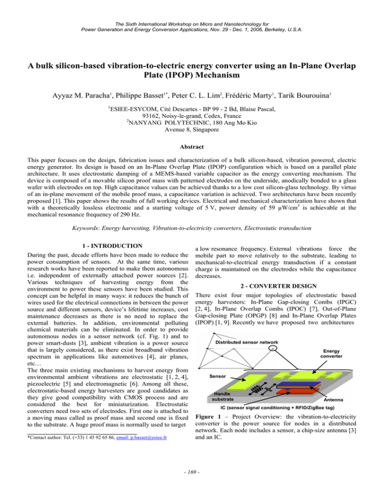
The Sixth International Workshop on Micro and Nanotechnology for Power Generation and Energy Conversion Applications, Nov. 29 - Dec. 1, 2006, Berkeley, U.S.A. A bulk silicon-based vibration-to-electric energy converter using an In-Plane Overlap Plate (IPOP) Mechanism Ayyaz M. Paracha1, Philippe Basset1*, Peter C. L. Lim2, Frédéric Marty1, Tarik Bourouina1 1 ESIEE-ESYCOM, Cité Descartes - BP 99 - 2 Bd, Blaise Pascal, 93162, Noisy-le-grand, Cedex, France 2 NANYANG POLYTECHNIC, 180 Ang Mo Kio Avenue 8, Singapore Abstract This paper focuses on the design, fabrication issues and characterization of a bulk silicon-based, vibration powered, electric energy generator. Its design is based on an In-Plane Overlap Plate (IPOP) configuration which is based on a parallel plate architecture. It uses electrostatic damping of a MEMS-based variable capacitor as the energy converting mechanism. The device is composed of a movable silicon proof mass with patterned electrodes on the underside, anodically bonded to a glass wafer with electrodes on top. High capacitance values can be achieved thanks to a low cost silicon-glass technology. By virtue of an in-plane movement of the mobile proof mass, a capacitance variation is achieved. Two architectures have been recently proposed [1]. This paper shows the results of full working devices. Electrical and mechanical characterization have shown that with a theoretically lossless electronic and a starting voltage of 5 V, power density of 59 µW/cm3 is achievable at the mechanical resonance frequency of 290 Hz. Keywords: Energy harvesting, Vibration-to-electricity converters, Electrostatic transduction 1 - INTRODUCTION During the past, decade efforts have been made to reduce the power consumption of sensors. At the same time, various research works have been reported to make them autonomous i.e. independent of externally attached power sources [2]. Various techniques of harvesting energy from the environment to power these sensors have been studied. This concept can be helpful in many ways: it reduces the bunch of wires used for the electrical connections in between the power source and different sensors, device’s lifetime increases, cost maintenance decreases as there is no need to replace the external batteries. In addition, environmental polluting chemical materials can be eliminated. In order to provide autonomous nodes in a sensor network (cf. Fig. 1) and to power smart-dusts [3], ambient vibration is a power source that is largely considered, as there exist broadband vibration spectrum in applications like automotives [4], air planes, etc… The three main existing mechanisms to harvest energy from environmental ambient vibrations are electrostatic [1, 2, 4], piezoelectric [5] and electromagnetic [6]. Among all these, electrostatic-based energy harvesters are good candidates as they give good compatibility with CMOS process and are considered the best for miniaturization. Electrostatic converters need two sets of electrodes. First one is attached to a moving mass called as proof mass and second one is fixed to the substrate. A huge proof mass is normally used to target __________________________________ *Contact author: Tel. (+33) 1 45 92 65 86, email: p.basset@esiee.fr a low resonance frequency. External vibrations force the mobile part to move relatively to the substrate, leading to mechanical-to-electrical energy transduction if a constant charge is maintained on the electrodes while the capacitance decreases. 2 - CONVERTER DESIGN There exist four major topologies of electrostatic based energy harvesters: In-Plane Gap-closing Combs (IPGC) [2, 4], In-Plane Overlap Combs (IPOC) [7], Out-of-Plane Gap-closing Plate (OPGP) [8] and In-Plane Overlap Plates (IPOP) [1, 9]. Recently we have proposed two architectures Distributed sensor network Energy converter Sensor Handle substrate Antenna IC (sensor signal conditioning + RFID/ZigBee tag) Figure 1 – Project Overview: the vibration-to-electricity converter is the power source for nodes in a distributed network. Each node includes a sensor, a chip-size antenna [3] and an IC. - 169 - The Sixth International Workshop on Micro and Nanotechnology for Power Generation and Energy Conversion Applications, Nov. 29 - Dec. 1, 2006, Berkeley, U.S.A. based on an IPOP topology [1], shown in Fig. 2. IPOP resembles to the concept of traditional parallel plate capacitor. As a result of lateral movement of the movable plate, there is a capacitive variation due to a change in the electrode’s overlap area. The devices are based on a silicon-glass technology [10]. Top electrodes are patterned on the back of the bulky silicon proof mass and lower electrodes are deposited on the glass wafer previously etched by HF. Then both the wafers are anodically bonded. By virtue of mechanical vibrations present in the environment, proof mass oscillates, hence the capacitance varies. The IPOP topology has the following advantages. Large value of maximum capacitance, due to small air gap between the sets of electrodes, leads to high power generation. Another convenience is the stability against out of axis vibration. It can be achieved by using a thick wafer, which increases the stiffness in the vertical direction. It reduces the complexity of the fabrication process, as the proposed designs do not have any closely spaced comb drive architecture. So tolerance of misalignment is relatively higher as compared to other topologies which have closely spaced comb electrodes. It also exhibits less fluid damping: as there is no compression of air, squeeze film damping is almost negligible. The basic difference between the two proposed designs is their proof mass. In the comb configuration (CC) 19 % of the total mass of silicon is removed from the space present in between the electrodes to reduce the parasitic capacitance. It results in reduction of overall mass of the device, hence increasing its natural frequency as compared to the proof mass configuration (PC) having the same dimensions. Fig. 3 shows FEM simulations of capacitive variation of the designs. Minimum capacitance (Cmin) of the energy harvester is composed of three components: the substrate parasitic capacitance (Csub), fringe field capacitance (Cff) between the two sets of electrodes and linear capacitance (Clin) which is a theoretical value. To reduce Cmin, Csub and Cff has to be minimized. Cmin’s value in PC is quite higher as compared to CC. Reducing 19% of total mass from PC, results in 25% reduction of Cmin in CC. But this mass reduction undesirably increases the resonance frequency of the device. So there should be find some compromise according to desired application. The non-linearities in the capacitance variations with displacements are due to the electrostatic fringe fields between top and bottom electrodes, as shown by the simulation of the capacitance’s variation of face-to-face aluminum electrodes. Cff can be reduced by designing different electrode’s width. However it is not desirable to have Cmin close to zero, because voltage will approach infinity and unwanted electrode stiction could occur. The last curve in Fig. 3 represents variation of Clin. It is calculated by the following analytical formula: Clin ( x) = N 2ε oε r LF (WF − x ) , t NIT + ε r g AIR (1) where N, εr, εo, LF, WF, tNIT, gAIR, and x are number of fingers, relative permittivity of dielectric, permittivity of free space, finger length, finger width, dielectric thickness, air gap present between two electrodes and lateral displacement of proof mass respectively. 3 - FABRICATION PROCESS The fabrication of the IPOP vibration-to-electricity converter involves parallel processing of the electrodes on a silicon and on a glass wafer, after which both of them are anodically bonded. Ordinary cheap 380 µm- thick 4" silicon and 500 µm-thick glass wafers are used. The fabrication steps are shown in Fig. 4. Deposition of a thermal oxide on the silicon wafer insulates it from the aluminum electrodes. A nitride is deposited on lower electrodes to serve as a passivation layer, to avoid unwanted stiction. The most important issue in the whole fabrication is the through-wafer DRIE process. At ESIEE, the silicon etching is performed [11] using AlcatelTM 601E plasma etcher. This equipment is configured with a 2 kW ICP source and RF or Low Frequency (LF) generator for the wafer polarization. The silicon wafer is clamped with a mechanical chuck and can be maintained at a temperature from -150 °C to +20 °C. To achieve the vertical anisotropic deep plasma etching, the Bosch process is used. For our device we need to etch the silicon through the whole wafer with pattern’s widths as small as 30 µm for the springs, besides big opening in the mm² size to Figure 2 - Proposed energy harvester design: a) comb configuration (CC), b) proof mass configuration (PC), [1] - 170 - The Sixth International Workshop on Micro and Nanotechnology for Power Generation and Energy Conversion Applications, Nov. 29 - Dec. 1, 2006, Berkeley, U.S.A. Al a) d) Glass Nitride e) b) Oxide c) Figure 3 - FEM simulation of capacitance variation for the two presented designs access the testing pads on the glass wafer. This is particularly critical because of the ARDE (Aspect Ratio Dependent Etching) effect. The high aspect-ratio of the structures is obtained using a specific mixed RF/LF pulsed process allowing smooth sidewall, perfect anisotropy and no negative effect of over-etching time. Fig. 5 shows the microscopic view of the silicon wafer’s back side after DRIE. It can be seen that the mechanical springs are fully released. The dark area shows the silicon dioxide from where the bulk silicon has been removed. Top view of the final device is shown in Fig. 6. 4 - CHARACTERIZATION Dimensions of the device without including the pads are 11 x 6.5 x 0.88 mm3. The device’s mechanical characterization has been done using a vibration table from Physik Instrumente tm. During the test, a sine wave is applied on the input of a dedicated current amplifier, generating a sinusoidal displacement of the table. While sweeping the frequency, the relative displacement of the structure’s proof mass had been observed with an optical profiler from Weeco tm. For an unbounded silicon wafer, the resonance frequency of the PC and CC is found to be 307 Hz, which is in accordance with the simulations done in Coventorwaretm. After the wafer bonding, the resonance frequency is found to be 290 Hz for the CC and 255 Hz for the PC. The decrease in resonance frequency is due to air being trapped in between the mobile and fixed parts after the bonding. The full wafer being excited with input amplitude of +/-5 µm, Fig. 7 shows, for the two designs, the maximum value of the relative displacement of proof mass versus frequency. Experimental values of Cmax and Cmin, when the potential of the silicon substrate is floating, are reported in Fig. 3. The maximum and minimum capacitances for the PC are 214 and 140 pF respectively. For CC, corresponding Cmax and Cmin are 214 and 80 pF. If substrate is grounded, most of the substrate parasitic capacitance is cancelled, so Cmax and Cmin in both cases are reduced by 33 pF. f) Silicon Figure 4 - Fabrication process - a) glass etching + sputtering of Al, b) PECVD nitride passivation, c) thermal oxidation + sputtering of Al-electrodes on silicon back side, d) Alsputtering of DRIE mask, e) through wafer DRIE, f) anodic bonding of substrate. The harvested energy, with an ideally lossless electronic, is given by the following equation [8]: ⎛C ⎞ 1 2 E = Vin (Cmax − Cmin )⎜⎜ max ⎟⎟ , 2 ⎝ Cmin ⎠ (2) where Vin is the starting voltage of the system. Power generated is calculated by multiplying the result of above equation with twice the resonance frequency, since in a single period the device capacitance reaches Cmin two times. For Vin equals to 5 V, the harvested power would be 0.72 and 2.6 µW for the PC and CC respectively, when the potential of the silicon substrate is floating. Hence the corresponding power densities for PC and CC are 11.26 and 40.62 µW/cm3 respectively. SiO2 Silicon beams Al electrodes on proof mass Figure 5 - Microscopic view of beams after DRIE of the silicon - 171 - The Sixth International Workshop on Micro and Nanotechnology for Power Generation and Energy Conversion Applications, Nov. 29 - Dec. 1, 2006, Berkeley, U.S.A. high aspectratio spring typical silicon wafer that is eventually bonded on a glass wafer. High capacitance density, due to the 1.5 µm vertical gap between the top and bottom electrodes, allows high energy conversion. Dimensions of the device without including the pads are 11 x 6.5 x 0.88 mm3. Maximum and minimum capacitance values are respectively 181 and 47 pF, if the silicon substrate is grounded. The harvested power density would be 59 µW/cm3 at 290 Hz, for a starting voltage of 5 V and a theoretically lossless electronic. The parasitic capacitance having a strong impact on the generated power, we have partially removed the silicon substrate on the proof mass to reduce it. This leads to an increase in the resonance frequency for a given area. As most common ambient vibrations are below 300 Hz, silicon should not be removed trough the whole wafer thickness in future designs. silicon partially removed to reduce the parasitic capacitance 380 µm pad on glass mechanical stopper 11 mm 6.5 mm mobile proof mass ACKNOWLEDGEMENTS vibration orientation Figure 6 - SEM pictures of vibration-to-electricity converter with two close-up views When substrate is grounded, the harvested power for CC becomes 3.74 µW, which corresponds to a power density of 59 µW/cm3. 5 - CONCLUSION We have presented a resonant electrostatic vibration-toelectricity converter using an In-Plane Overlap Plate topology. Batch CMOS-compatible process is performed on a Figure 7 - Maximum relative displacement of proof mass versus frequency for a sinusoidal input excitation with 5 µm peak amplitude Authors would like to thank the SMM team in ESIEE for their extensive cooperation during the fabrication process in the clean room. Also special thanks to Dr P. Poulichet and his students, Mr. J. Rouessard and Mr. Y. Guo, for fabricating the test circuit board. This work is partially funded by the French Research Agency (ANR, Agence Nationale pour la Recherche) and is supported by the French competitiveness cluster "Ville et Mobilité Durable". REFERENCES [1] P. Lim et al., “Design of a novel highly capacitive MEMS-based vibration to electricity energy converter with suspended in-plane overlap technology”, Proc. of APCOT’06, Singapore, 2006 [2] S. Roundy et al., “Micro-electrostatic vibration-to-electricity converters”, Proc. of IMEC’02, New Orleans, USA, 2002 [3] P. Basset et al., “Chip-size antennas for implantable sensors and smart dusts”, Proc. of Transducers’05, Seoul, Korea, 2005 [4] G. Despesse et al., “Fabrication and Characterization of High Damping Electrostatic Micro Devices for Vibration Energy Scavenging”, Proc. of DTIP’05, pp. 386-390, 2005 [5] M. Marzencki et al., “Design and fabrication of piezoelectric micro power generators for autonomous microsystems”, Proc. of DTIP’05, pp. 299-302, 2005 [6] P. Glynne-Jones et al., “An electromagnetic, vibration-powered generator for intelligent sensor systems”, Sensors and Actuators, vol. A 110, pp. 344-349, 2004 [7] S. Meninger et al., “Vibration-to-electric energy conversion”, IEEE Trans. on VLSI, vol. 9, no. 1, pp. 64-76, 2001 [8] P. Miao et al., “Micro-machined variable capacitors for power generation”, Proc. of Electrostatic’03, 2003 [9] T. Sterken et al., “Motion based generators for industrial applications”, Proc. of DTIP’06, 2006 [10] C. M. Tassetti et al., “New tunable RF MEMS Microinductor design”, Journal of Micromechanics and Microengineering, vol. 14, no. 9, pp. 17-22, 2004 [11] F. Marty et al., “Advanced etching based on deep reactive ion etching for silicon high aspect ratio microstructures and three dimensional micro and nano structures”, Microelectronics journal, vol. 36, pp. 673-677, 2005 - 172 -


