A 30 Year Retrospective on Dennard's MOSFET Scaling Paper
advertisement
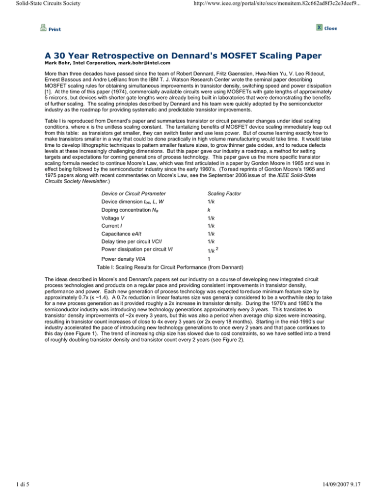
Solid-State Circuits Society http://www.ieee.org/portal/site/sscs/menuitem.82c662ad8f3c2e3deef9... A 30 Year Retrospective on Dennard's MOSFET Scaling Paper Mark Bohr, Intel Corporation, mark.bohr@intel.com More than three decades have passed since the team of Robert Dennard, Fritz Gaensslen, Hwa-Nien Yu, V. Leo Rideout, Ernest Bassous and Andre LeBlanc from the IBM T. J. Watson Research Center wrote the seminal paper describing MOSFET scaling rules for obtaining simultaneous improvements in transistor density, switching speed and power dissipation [1]. At the time of this paper (1974), commercially available circuits were using MOSFETs with gate lengths of approximately 5 microns, but devices with shorter gate lengths were already being built in laboratories that were demonstrating the benefits of further scaling. The scaling principles described by Dennard and his team were quickly adopted by the semiconductor industry as the roadmap for providing systematic and predictable transistor improvements. Table I is reproduced from Dennard’s paper and summarizes transistor or circuit parameter changes under ideal scaling conditions, where is the unitless scaling constant. The tantalizing benefits of MOSFET device scaling immediately leap out from this table: as transistors get smaller, they can switch faster and use less power. But of course learning exactly how to make transistors smaller in a way that could be done practically in high volume manufacturing would take time. It would take time to develop lithographic techniques to pattern smaller feature sizes, to grow thinner gate oxides, and to reduce defects levels at these increasingly challenging dimensions. But this paper gave our industry a roadmap, a method for setting targets and expectations for coming generations of process technology. This paper gave us the more specific transistor scaling formula needed to continue Moore’s Law, which was first articulated in a paper by Gordon Moore in 1965 and was in effect being followed by the semiconductor industry since the early 1960’s. (To read reprints of Gordon Moore’s 1965 and 1975 papers along with recent commentaries on Moore’s Law, see the September 2006 issue of the IEEE Solid-State Circuits Society Newsletter.) Device or Circuit Parameter Device dimension tox, L, W Scaling Factor Doping concentration Na k Voltage V Current I Capacitance eA/t Delay time per circuit VC/I 1/k 1/k 1/k 1/k Power dissipation per circuit VI 1/k 2 Power density VI/A 1 1/k Table I: Scaling Results for Circuit Performance (from Dennard) The ideas described in Moore’s and Dennard’s papers set our industry on a course of developing new integrated circuit process technologies and products on a regular pace and providing consistent improvements in transistor density, performance and power. Each new generation of process technology was expected to reduce minimum feature size by approximately 0.7x ( ~1.4). A 0.7x reduction in linear features size was generally considered to be a worthwhile step to take for a new process generation as it provided roughly a 2x increase in transistor density. During the 1970’s and 1980’s the semiconductor industry was introducing new technology generations approximately every 3 years. This translates to transistor density improvements of ~2x every 3 years, but this was also a period when average chip sizes were increasing, resulting in transistor count increases of close to 4x every 3 years (or 2x every 18 months). Starting in the mid-1990’s our industry accelerated the pace of introducing new technology generations to once every 2 years and that pace continues to this day (see Figure 1). The trend of increasing chip size has slowed due to cost constraints, so we have settled into a trend of roughly doubling transistor density and transistor count every 2 years (see Figure 2). 1 di 5 14/09/2007 9.17 Solid-State Circuits Society http://www.ieee.org/portal/site/sscs/menuitem.82c662ad8f3c2e3deef9... Figure 1: Feature size scaling for Intel logic technologies Figure 2: Transistor count trend for Intel microprocessors Even more surprising, from a MOSFET scaling perspective, is that over the past 10 years MOSFET gate lengths have been scaling faster than other minimum feature sizes (see Figure 1). Prior to the mid-1990’s, gate lengths were roughly the same size as other minimum process features, but starting with the 0.35 mm generation, gate lengths have been scaling faster than 0.7x per generation to realize performance advantages, even though gate pitch has been scaling at the normal rate. This has been a key factor in microprocessors achieving >3 GHz operating frequencies sooner than most experts thought possible even 10 years ago. It is exciting to see in Figure 3 how far we have taken Dennard’s scaling law by comparing the 1 mm transistor described in his 1974 paper to the 35 nm gate length transistor used in Intel’s 65 nm generation logic technology that started high volume manufacturing in 2005 [2]. The Intel transistor shown in Figure 3 provides an example of an emerging trend among semiconductor manufacturers: the introduction of new structures and materials to extend transistor scaling. In this case the new feature is selectively deposited SiGe source-drains to provide strained silicon for improved transistor performance [3]. Physical Gate Length Electrical Channel Length Gate Oxide Thickness Channel Doping 2 di 5 >1.0 mm 1.0 mm 35 nm 4x1016 cm-3 4.0 V 35 nm <20 nm 1.2 nm ~1018 cm-3 1.2 V 14/09/2007 9.17 Solid-State Circuits Society http://www.ieee.org/portal/site/sscs/menuitem.82c662ad8f3c2e3deef9... Operating Voltage Figure 3: MOSFET structure from Dennard’s 1974 paper (left) and from Intel’s 65 nm generation logic technology in 2005 (right) Just as there have been questions about the end of Moore’s Law, there have also been questions about the end of MOSFET scaling. In both cases, the answer is that the end is not yet in sight, although we face growing challenges in their continuation. Voltage scaling has been an extremely important component of MOSFET scaling because it maintains constant electric field, which is important for reliability, and it lowers transistor power, which is needed to maintain constant power density. But even in the early days of MOSFET scaling it was difficult to follow ideal voltage scaling requirements because of the need to use industry standard voltages, such as 12V, 5V, 3.3V, etc. Eventually we were able to deviate from standard voltage levels on key products such as microprocessors and were free to adjust product voltage levels to meet specific performance and power targets. More recently, however, voltage scaling has run into lower limits imposed by threshold voltage (VT) scaling limits [4]. Dennard’s scaling law assumed that VT would scale along with operating voltage, and thus provide improved performance and power. But this 1974 work ignored the impact of transistor sub-threshold leakage on overall chip power. Sub-threshold leakage was relatively low in the 1970’s and was a tiny contributor to total power consumption on logic circuits. But after 30 years of scaling, VT has scaled to the point where sub-threshold leakage has increased from levels of <10-10 amps/mm to >10-7 amps/mm. Due to leakage constraints, it will be difficult to further scale VT and thus it will also be difficult to scale operating voltage. Another key assumption in Dennard’s scaling law was the ability to scale gate oxide thickness. Gate oxide scaling has been a key contributor to scaling improvements over the past 30 years, but this trend is also slowing due to leakage constraints (see Figure 4). Intel’s 65nm generation transistors use a SiO2 gate dielectric with a thickness of 1.2 nm [2]. This dielectric is only about 5 silicon atomic layers thick and represents what is likely the limit to which SiO2 can be scaled. Not only are we running out of atoms, but gate oxide leakage due to direct tunneling current is becoming a noticeable percentage of overall chip power. Figure 4: Gate oxide thickness trend for Intel logic technologies Dennard’s scaling law assumed that channel doping concentration could be continually increased to enable shorter channel lengths with the appropriate VT. When channel doping concentration gets too high two problems occur: 1) carrier mobility and performance degrade due to increased impurity scattering, 2) source and drain junction leakage increases due to direct band-band tunneling. Junction leakage is already a limiter for ultra-low power integrated circuits and will eventually be a limiter for mainstream microprocessor products. Although Dennard’s paper is best known for articulating MOSFET scaling rules, less noticed was the paper’s description of interconnect scaling results, as reproduced here in Table II. The key point of this table is that scaled interconnects, unlike scaled transistors, do not speed up. Scaled interconnects provide roughly constant RC delays because the reduction in line capacitance is offset by an increase in line resistance. This was not much of a concern in 1974 when interconnect delay was typically a small portion of circuit clock cycle times. But more modern logic technologies have been wrestling with the constraints imposed by interconnect delay and interconnect density [5], and have been addressing these constraints by adding more metal layers, converting from aluminum to more conductive copper wires, and replacing SiO2 dielectrics with low- dielectrics to reduce capacitance (see Figure 5). Parameter Line resistance, RL =L/Wt Normalized voltage drop IRL/V Line response time RLC Line current density I/A 3 di 5 Scaling Factor 1 14/09/2007 9.17 Solid-State Circuits Society http://www.ieee.org/portal/site/sscs/menuitem.82c662ad8f3c2e3deef9... Table II: Scaling Results for Interconnect Lines (from Dennard) Figure 5: Copper interconnects with low- dielectrics from Intel’s 65 nm logic technology As briefly described above, scaling transistors beyond the 65 nm generation will clearly have more challenges to contend with. It is also commonly recognized that following the simple scaling rules described by Dennard and his team back in 1974 is now no longer a sufficient strategy to meet future transistor density, performance, and power requirements. But ours is a very inventive industry and new transistor technologies such as strained silicon, high- dielectrics, metal gates and multiple-gate devices have been or will be introduced to continue scaling. So although the letter of “Dennard’s Law” can no longer be followed, it has gotten us very far over the past 30 years and the spirit is alive and well in transistor R&D facilities around the world. REFERENCES [1] R. Dennard, et al., “Design of ion-implanted MOSFETs with very small physical dimensions,” IEEE Journal of Solid State Circuits, vol. SC-9, no. 5, pp. 256-268, Oct. 1974. [2] P. Bai, et al., “A 65nm logic technology featuring 35nm gate lengths, enhanced channel strain, 8 Cu interconnect layers, low-k ILD and 0.57 mm2 SRAM cell,” International Electron Devices Meeting Technical Digest, pp. 657-660, 2004. [3] K. Mistry, et al., “Delaying forever: Uniaxial strained silicon transistors in a 90nm CMOS technology,“ Symposium on VLSI Technology Digest of Technical Papers, pp. 50-51, 2004. [4] Y. Taur and E. Nowak, “CMOS devices below 0.1 mm: How high will performance go?“ International Electron Devices Meeting Technical Digest, pp. 215-218, 1997. [5] M. Bohr, “Interconnect scaling - The real limiter to high performance ULSI,” International Electron Devices Meeting Technical Digest, pp. 241-244, 1995. About the Author Mark Bohr is an Intel Senior Fellow and Director of Process Architecture and Integration. He is a member of Intel’s Logic Technology Development group located in Hillsboro, Oregon, where he is responsible for directing process development activities for Intel’s advanced logic technologies. He joined Intel in 1978 and has been responsible for process integration and device design on a variety of process technologies for dynamic RAM, static RAM and microprocessor products. He is currently directing development activities for Intel's 32 nm logic technology. 4 di 5 14/09/2007 9.17 Solid-State Circuits Society http://www.ieee.org/portal/site/sscs/menuitem.82c662ad8f3c2e3deef9... Bohr was born in Chicago, Illinois in 1953. He received the B.S. degree in industrial engineering in 1976 and the M.S. degree in electrical engineering in 1978, both from the University of Illinois, Urbana-Champaign. In 1998 he received the Distinguished Alumnus Award from the University of Illinois department of Electrical and Computer Engineering. Bohr is a Fellow of the Institute of Electrical and Electronics Engineers and was the recipient of the 2003 IEEE Andrew S. Grove award. In 2005 he was elected to the National Academy of Engineering. He holds 42 patents in the area of integrated circuit processing and has authored or co-authored 40 published papers. From the January 2007 Issue Printed from: http://www.ieee.org/portal/pages/sscs/07Winter/Bohr.html 5 di 5 14/09/2007 9.17


