Characterization and Properties New Materials for 157 nm Photoresists:
advertisement
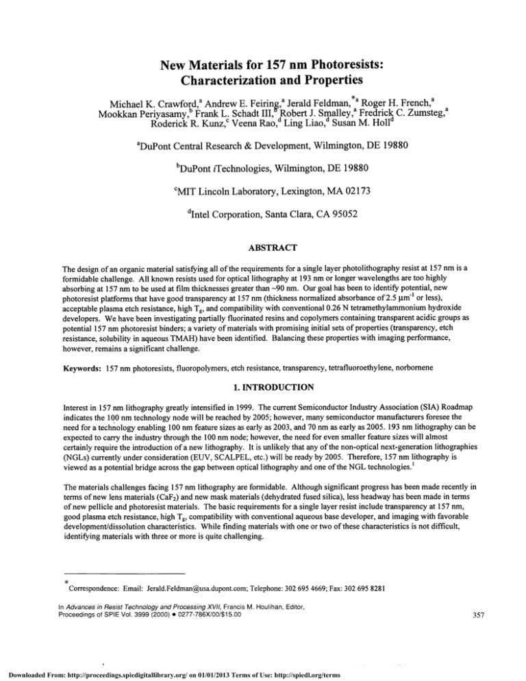
New Materials for 157 nm Photoresists: Characterization and Properties Michael K. Crawford,a Andrew E. Feirin Jerald Feldman,* Roger H. French,a Mookkan Periyasamy," Frank L. Schadt III, Robert J. Smalley,a Fredrick C. Zumsteg,a Roderick R. Kunz,C Veena Rao,d Ling Liao,' Susan M. HoW' aDupont Central Research & Development, Wilmington, DE 19880 bDuPont iTechnologies, Wilmington, DE 19880 eMIT Lincoln Laboratory, Lexington, MA 02173 dlntel Corporation, Santa Clara, CA 95052 ABSTRACT The design ofan organic material satisfying all ofthe requirements for a single layer photolithography resist at 157 nm is a formidable challenge. All known resists used for optical lithography at 193 nm or longer wavelengths are too highly absorbing at 157 nm to be used at film thicknesses greater than -9O nm. Our goal has been to identify potential, new photoresist platforms that have good transparency at 157 nm (thickness normalized absorbance of2.5 rim' or less), acceptable plasma etch resistance, high Tg, and compatibility with conventional 0.26 N tetramethylammonium hydroxide developers. We have been investigating partially fluorinated resins and copolymers containing transparent acidic groups as potential 157 nm photoresist binders; a variety ofmaterials with promising initial sets ofproperties (transparency, etch resistance, solubility in aqueous TMAH) have been identified. Balancing these properties with imaging performance, however, remains a significant challenge. Keywords: 1 57 nm photoresists, fluoropolymers, etch resistance, transparency, tetrafluoroethylene, norbornene 1. INTRODUCTION Interest in 157 nm lithography greatly intensified in 1999. The current Semiconductor Industry Association (SIA) Roadmap indicates the 100 nm technology node will be reached by 2005; however, many semiconductor manufacturers foresee the need for a technology enabling 100 nm feature sizes as early as 2003, and 70 nm as early as 2005. 193 nm lithography can be expected to carry the industry through the 1 00 nm node; however, the need for even smaller feature sizes will almost certainly require the introduction ofa new lithography. It is unlikely that any ofthe non-optical next-generation lithographies (NGLs) currently under consideration (EUV, SCALPEL, etc.) will be ready by 2005. Therefore, 157 nm lithography is viewed as a potential bridge across the gap between optical lithography and one ofthe NGL technologies.' The materials challenges facing 157 nm lithography are formidable. Although significant progress has been made recently in terms of new lens materials (CaF2) and new mask materials (dehydrated fused silica), less headway has been made in terms of new pellicle and photoresist materials. The basic requirements for a single layer resist include transparency at 1 57 nm, good plasma etch resistance, high Tg, compatibility with conventional aqueous base developer, and imaging with favorable development/dissolution characteristics. While finding materials with one or two of these characteristics is not difficult, identifying materials with three or more is quite challenging. * Correspondence: Email: Jerald.Feldman@usa.dupont.com; Telephone: 302 695 4669; Fax: 302 695 8281 In Advances in Resist Technology and Processing XVII, Francis M. Houlihan, Editor, Proceedings of SPIE Vol. 3999 (2000) • 0277-786X!00I$15.0O Downloaded From: http://proceedings.spiedigitallibrary.org/ on 01/01/2013 Terms of Use: http://spiedl.org/terms 357 Past experience indicates that although fluorinated materials may provide some unique advantages with respect to transparency at very short wavelengths, they also introduce difficulties with regard to aqueous base solubility. The plasma etch resistance of fluorinated materials has not been extensively explored. We have been investigating hydrofluorocarbon resins as potential 157 nm photoresist platforms, with the objective of identifying materials that optimize the properties described above. 2. EXPERIMENTAL Caution! One ofthe monomers used to synthesize the materials described below is tetrafluoroethylene (TFE), a deflagrating explosive and an experimental carcinogen. All work with TFE described in this report was conducted within completely barricaded and ventilated facilities. Assessment of 157 nm imaging sensitivity was done using a Lambda-Physik Compex 102 excimer laser configured for 1 57nm operation. Vacuum ultraviolet transmission measurements were made using either an Acton or a McPherson spectrometer equipped with a D2 light source. Samples were spin-coated at several thicknesses on CaF2 substrates, and the contribution ofthe substrate to the transmission was approximately removed by spectral division. Resist dissolution was characterized after exposure at 248 nm or 1 57 nm using a commercial resist dissolution rate analyzer. 1 57 nm exposures were performed using a 157 nm 0.5 NA microstepper equipped with Schwartzchild optics at Intel. Top-down SEM micrographs were taken with an intermediate voltage high resolution CD SEM. 3. RESULTS AND DISCUSSION 3.1. Copolymers of norbornene with tetrafluoroethylene Previous work has demonstrated that all known photoresist platforms are too highly absorbing at 157 nm to be used at film thicknesses greater than —9O nm; i.e. they would have to be employed as ultra-thin films at 157 nm.2 Our first goal was to identify materials that would be much more transparent to 157 nm light than conventional photoresists, but maintain high plasma etch resistance. Since transparency considerations clearly precluded the use ofaromatic groups to impart etch resistance to a 1 57 nm resist, we turned our attention to partially fluorinated resins containing multicyclic groups.3 Tetrafluoroethylene (TFE) is an electron-deficient olefin and undergoes free-radical copolymerization with norbornene (NB) to give resins that we found to be transparent, thermally stable, and plasma etch resistant (eq 1). NB/TFE copolymers are .CF2— CF2=CF2 + (1) typically low molecular weight (Mn 2,000 - 6,000) and approximately alternating. They are readily soluble in organic solvents, have high glass transition temperatures, are very transparent at 193 nm, and have good plasma etch resistance (see below). However, unlike poly(NB/maleic anhydride), polynorbornene, and other DUV and 193 nm resist platforms, they also possess reasonably good transparency at 157 nm (Table 1). Thus, poly(NB/TFE) would appear to be a promising platform for a 157 nm photoresist binder. 358 Downloaded From: http://proceedings.spiedigitallibrary.org/ on 01/01/2013 Terms of Use: http://spiedl.org/terms Table 1. Comparison ofpoly(NBITFF' "' (157 nm with other resins Abs Coefficient Polymer entry @_157_nm_(jim1) 1 2 3 4 5 6 7 8 7-8 5.7 6.7 11.0 Commercial DUV Resists (phenolic) Poly(methyl methacrylate) Poly(norbornyl methacrylate) Poly(acrylicacid) Poly(norbomene) - unfunctionalized ROMP Poly(norbornene) - hydrogenated Poly(norbomene-alt-maleic anhydride) Poly(tetrafluoroethylene/norbornene) 6-7 6.8 8-9 1.3 Of course, any photoresist material must contain suitable functionalities for adhesion, aqueous-base development, etc. Therefore, it was of interest to synthesize functionalized derivatives ofpoly(NB/TFE), and evaluate their physical properties. Terpolymers and tetrapolymers incorporating functional groups (e.g. acetates and carboxylic acids/esters) were synthesized. Table 2 provides absorption and etch rate data on several NB/TFE copolymers incorporating vinyl acetate, tert-butyl acrylate, and 5-norbornene-2-carboxylic acid tert-butyl ester; typical UV absorption spectra are shown in Figures 1 and 2. ' Table 2. 1th rate (CFdO) -- and 2hnrntinn () 1 7 nm) dt fhr N1/TPE nnn1vmerc Relative Abs Coefficient entry Polymer' @ 157 nm (j.tm') Etch Rate2 --1 Novolak Resin (Borden) 1.0 2 3 4 1.2 1.3 TFE(49%)/NB (51%) 2.0 1 .3 TFE (41%) /NB (46%)/VA (12%) 2. 1 1 .5 TFE (43%) INB (38%)/VA (20%) 5 2.6 1 .6 TFE (43%) /NB (28%)IVA (29%) 1 .2 6 2.4 TFE (36%) /NB (47%)/TBA (17%) 7 3.6 1.4 TFE (28%)INB (38%)/TBA (34%) 8 not determined j 1.4 TFE (42%) /NB (41%)/NB-CO2tBu (17%) I TFE = Tetrafluoroethylene, NB Norbornene, VA Vinyl Acetate, TBA tert-Butyl Acrylate, . Tg (°C) Mn; Mw/Mn --- --- 151 1,700; 1.6 4,300; 3.8 6,300; 2.4 7,900; 2.8 5,600; 2.0 7,500; 2.2 4,300; 3.8 124 101 92 130 115 171 NBCO2tBu = 5-norbornene-2-carboxylic acid tert-butyl ester 2Etch data (CF4/02 plasma, 40/7.lsccm, 150 mtorr, 300 W, 483 V DC Bias) It can be seen from Table 2 that poly(NB/TFE) itself has good etch resistance relative to a Novolak resist in a CF4/02 plasma. The etch resistance ofpoly(NBITFE) was also evaluated relative to a poly(para-hydroxystyrene) (PHOST) based DUV resist. In an HBr/C12 polysilicon etch, poly(NB/TFE) etches at 0.8x the rate ofthe PHOST-DUV resist. In a more aggressive oxide etch, poly(TFE/NB) etches at 0.9x the rate ofthe PHOST-DUV resist. Thus, the etch resistance ofpoly(NBiTFE) is wellestablished. 359 Downloaded From: http://proceedings.spiedigitallibrary.org/ on 01/01/2013 Terms of Use: http://spiedl.org/terms w 12 0 10 0 08 06 0. 0(I) .0 0 130 150 170 190 Wavelength (nm) Fig 1. UV spectrum of tetrafluoroethylene/norbornene (52:48) copolymer 10 0 o8 C) C .2 6 0. I.. 0 U) .0 i. 0 130 150 170 190 Wavelength (nm) Fig 2. UV spectrum of tetrafluoroethylene/norbornene/vinyl acetate (43:38:20) copolymer 360 Downloaded From: http://proceedings.spiedigitallibrary.org/ on 01/01/2013 Terms of Use: http://spiedl.org/terms Not surprisingly, etch-rates increase as oxygen-containing functionality is incorporated into the polymer.4 Nevertheless, up to —25 mol% ester or acetate functionality can be introduced into the polymer while maintaining reasonable plasma etch resistance (etch rate <1.5x Novolak). Absorption at 157 nm also increases with increasing carbonyl content, although it is interesting to note that a NB/TFE copolymer containing -3O mol% ester or acetate is significantly less absorbing (3.6 rim') than unfunctionalized polynorbornene (6-7 rim'). Terpolymers of TFE, norbornene, and tBu acrylate were found to function as negative resists, when formulated with a photoacid generator, exposed to broad band UV radiation, and developed in an organic solvent (e.g. chlorobenzene). Although NB/TFE copolymers containing <30 mol% ester (i.e. with reasonable transparency at 157 nm) will give positive images using 0.262 N aqueous tetramethylammonium hydroxide (TMAH) developer, the resist in areas exposed to light is not removed uniformly through conventional dissolution, but rather non-uniformly through mechanisms involving various combinations ofcracking, swelling or preferential dissolution in multiphase systems. Clearly, some amount of carboxylic acid/ester can be incorporated into the polymer backbone while maintaining reasonable transparency at 157 nm; however, these functionalities cannot be incorporated at high enough levels to enable dissolution without severely impacting transparency. Therefore, there is a need for alternative acidic functional groups that are much more transparent to 1 57 nm light than the phenols and carboxylic acids that, until now, have been ubiquitous in UV-sensitive photoresists.5 3.2. Other Potential 157 nm Photoresist Platforms More generally, what is required for a 1 57 nm photoresist is a binder that is some combination of a transparent, etch resistant backbone (e.g. NB/TFE), a transparent acidic functional group, and an acid-catalyzed solubility switch. Thus, we have broadly surveyed many different polymer backbones and polar functional groups in a search for materials that balance transparency, etch resistance, and aqueous base solubility. Table 3 provides plasma etch and 1 57 nm absorption data for six different polymers in three different polymer families (i.e. polymers Al and A2 are closely related structurally, as are polymers Bi and B2, and Cl and C2). All ofthese materials have substantially better transparency at 157 nm than known photoresist platforms (cf. Table 1); nevertheless, several have sufficient functionality to dissolve in 0.262 N TMAH. The polymer backbones can be made more or less etch resistant, but not without affecting other key properties. Table 3. Oxide etch rate and absorption ((l57 nm) data for fluoropolymers A2 Soluble in 0.262 N TMAH? Yes Yes (when deprotected) Bi Yes B2 No Polymer Al Cl No C2 Yes Abs Coefficient @ 157 nm (j.tm') — — — 3.0 4.1 Etch Rate1 (vs. Novolak) 1.6 1.2 1.0 3.6 3.4 3.4 2.9 1.2 not determined 1.6 I Oxygen plasma For example, polymer Al is base-soluble and has reasonably good transparency at 157 nm, but it has mediocre etch resistance. The etch resistance ofthis material can be significantly improved by incorporation ofan additional multicyclic monomer containing an acid-catalyzed solubility switch. Thus, polymer A2 etches at only 1 .2x the rate ofNovolak and is still soluble in 0.262 N TMAH (when deprotected). However, the absorbance at 157 nm for A2 is higher than that ofAl. This example illustrates one ofthe balancing acts at 157 nm (Figure 3): in this case, etch resistance and contrast come with a price in transparency. 361 Downloaded From: http://proceedings.spiedigitallibrary.org/ on 01/01/2013 Terms of Use: http://spiedl.org/terms Transparency Base Solubility Transparency Etch, Tg Etch, T Base Solubility A Fig 3. Balancing photoresist properties at 157 nm Polymer Bi is a fluoropolymer that is soluble in 0.262 N TMAH and has remarkably good transparency at 157 nm. However, it has an extremely high etch rate in an oxygen plasma. We found we could dramatically improve the etch resistance ofthis resin by appending multicyclic groups to the polymer backbone (polymer B2). B2 etches at less than half the rate of Bi; however, it is not soluble in 0.262 N TMAH and, surprisingly, is much less transparent at 157 nm. Thus, etch resistance has to be balanced with aqueous base solubility and transparency, at least in this system. Polymer Cl is not soluble in 0.262 N TMAH and has mediocre transparency at 157 nm, but it has very good plasma etch resistance. We found that by copolymerizing in a small amount of a transparent, acidic functional group we could arrive at a composition (polymer C2) which is soluble in 0.262 N TMAH and has reasonably good transparency at 157 nm. Yet another property that needs to be considered in terms of its impact on others is glass transition temperature (Tg). Figure 4 shows a plot OfTg as a function ofthe mole fraction ofa transparent, acidic functional group in a series of fluoropolymers. When no acidic group is present, the fluoropolymer possesses high Tg, but is insoluble in 0.262 N TMAH. Acidic groups can be appended to the polymer in order to reach a composition which dissolves in aqueous base; however, as shown in Figure 4, Tg also rapidly drops off with increasing acid content in this system. 140 120 1 00 Tg 80 60 40 20 0 0 0.1 0.2 0.3 0.4 0.5 mole fraction acidic group Fig 4. Plot of glass transition temperature (°C) as a function of transparent, acidic group content 362 Downloaded From: http://proceedings.spiedigitallibrary.org/ on 01/01/2013 Terms of Use: http://spiedl.org/terms More generally, we have found that the physical properties that need to be balanced at 157 nrn are those shown in Figure 3. Functional groups that are good for aqueous base soluhility, such as phenols and carboxylic acids, arc bad for transparency at 157 nm. Functional groups that are good for transparency and aqueous base solubility (e.g. fluorinated alcohols), can degrade etch resistance. This is probably due to the fact that most functional groups that are relatively transparent at 157 urn are saturated.4 Monomers that are good for etch resistance and T,, such as multicyclic monomers, work against aqueous base solubility and can be surprisingly bad for transparency at I 57 urn as well. 3.3. Imaging at 157 nm All of the work described above assumes that a 157 nrn resist will behave functionally in the same manner as chemically amplified resists do at 93 nm and 248 nm. l'hat is, the formulation will include some amount of acid functionality to impart solubility in an aqueous base developer (i.e. 0.262 N TMAH). Some fraction of the acid groups will he protected, which prevents polymer solubility until those groups have been cleaved off (deprotected) and replaced by H atoms. Deprotection is accomplished by incorporating a few weight percent of a photoacid generator (FAG), which absorbs the incident light at the lithographic wavelength and then converts to an acid that deprotects the polymer. Each photon absorbed may activate at most one PAG molecule, but each activated PAG will then catalytically cleave up to several hundred protecting groups, hence the term chemical amplification. The chemical amplification must occur at an elevated temperature (not at room temperature), but yet have an activation energy which is not too high since the post exposure bake step is expected to require only one to two minutes at temperatures in the vicinity of 100 C. Clearly, the polymer must remain stable and rigid during this baking step to maintain the required very high spatial resolution (on the order of 100 nm) of the image. Figure 5. SEM images of a candidate resist imaged with the 0.5 NA 157 nm microsiepper at mid. The film is 153 nm thick. 'flie image on the left is about 15 pm across, while that on the right is about 60 pm across. The image on the left shows 0.35 pm nested elbows. To evaluate the imaging properties of these polymers. various formulations incorporating the polymer, various PAG's and protected dissolution inhibitors were prepared. Initial assessment of 157 urn imaging was done using a Lambda-Physik Compex 102 excimer laser configured for 157nm operation. Imaging consisted of making open-frame exposures using varying numbers of pulses. Preliminary tests show that formulations using these polymers can be made that produce developable images in coatings as thick as 250-nm with laser fluences as low as 10 mi/cm2. Further evaluation of imaging and development mechanisms was done using the 0.5 NA 157 urn microstepper at Intel. Figure 5 shows SEM images of a mask pattern created using 1 57 nm light in a prototype resist with a thickness of 153 nm. A standard TMAH developer was used. Some features with sizes below one .ini are resolved, although there is considerable line edge roughness in the image. possibly as the result of non-homogeneous dissolution. I'he nested elbows in the image to the left have a spacing of 0.35 pm. Measurement of resist sensitivity (dose—to-clear) yielded a value near 20 mi/cm2. This is particularly significant in that many of these formulations have near goal etch resistance, but varying amounts of optical absorption. For example, the formulated 157 nm (hut still lower resist used to create the image shown in Figure 5 has a rather high absorption coefficient of 5 .im' than most of the systems in Table 1), and etch resistance comparable to deep UV resists (I Ox P1-lOST in an oxide etch I .2x P1-lOST in a polysilicon etch). Downloaded From: http://proceedings.spiedigitallibrary.org/ on 01/01/2013 Terms of Use: http://spiedl.org/terms 4. SUMMARY AND CONCLUSIONS Designing a single-layer photoresist for 157 nm is an exciting challenge for the resist chemist. Balancing key properties such as plasma etch resistance, aqueous base solubility, and transparency - properties that often seem to be in conflict with one another - is probably more difficult at 157 nm than at longer wavelengths. Certainly the number of options in the resist chemist's "tool box," e.g. optically transparent polymer backbones and functional groups, appears to be more limited at 157 nm than at other wavelengths. Nevertheless, there is reason to believe that a single-layer 157 nm photoresist is feasible. For example, fluoropolymers and fluorine-containing functional groups have reasonable transparency at 1 57 nm. The work described in this paper demonstrates that fluoropolymers can be made compatible with aqueous tetramethylammonium hydroxide, the industry's standard developer. Moreover, we have shown that fluoropolymers can be plasma etch resistant. For example, functionalized norbomene/TFE copolymers have etch resistances comparable to those ofDUV resists. Thus, there doesn't appear to be anything intrinsically "wrong" with fluoropolymers as photoresist platforms, at least as far as aqueous base solubility and etch resistance are concerned. The preliminary results for various fluoropolymers shown here, although encouraging, show that better optimization of their dissolution properties, transparency and adhesion are necessary to develop photoresists for 157 nm lithography. As noted above, we have identified materials with good etch resistance that, with coatings as thick as 250 nm, will give images upon exposure to 157 nm light, followed by development in 0.262 N TMAH. Nevertheless, maintaining etch resistance and increasing transparency, while optimizing the resist to achieve high resolution and other key properties (e.g. edge sharpness, contrast, adhesion), clearly presents a very significant challenge. 5. ACKNOWLEDGMENTS We thank the following for their assistance with this work: Mary Blasko, Brian Fischel, Mark Guidry, Ying He, Dave Jones, Bob Lewis, Betsy McCord, Vince Neal, Mark Ramsdell, Bob Smith, Carole Urbston-Meth, Bill Wheeler, and Ed Wonchoba (DuPont); Eric Panning, Ben Delos Reyes and Janet Chambers (Intel). We thank Dr. Michael Fryd for helpful discussions, and Curt Fincher for guidance, encouragement, and leadership. This work does not constitute an Intel endorsement of any product or supplier. The Lincoln Laboratory portion ofthis work was sponsored by the Advanced Lithography Program of the Defense Advanced Research Projects Agency under Air Force Contract F19628-95-C-0002. Opinions, interpretations, conclusions, and recommendations are those ofthe authors and are not necessarily endorsed by the United States Government. 6. REFERENCES 1. J. A. McClay and A. S. L. McIntyre, "157 nm optical lithography: the accomplishments and the challenges," Solid State Technology, June 1999, p.57 2. R. R. Kunz, T. M. Bloomstein, D. E. Hardy, R. B. Goodman, D. K. Downs, and J. E. Curtin, "Outlook for 157-nm resist design," Proc. 5P1E3678, 13 (1999). 3. Several 193 nm photoresist platforms incorporate multicyclic groups into the polymer backbone, since aromatic groups (which impart etch resistance to 248 nm resists) are strongly absorbing at 193 nm; see: (a) E. Reichmanis, 0. Nalamasu, and F. M. Houlihan, "Organic materials challenges for 193 nm imaging," Acc. Chem. Res. 32, 659 (1999); (b) U. Okoroanyanwu, 1. Shimokawa, J. D. Byers, and C. G. Willson, "Pd(II)-catalyzed addition polymerization and ring opening metathesis polymerization of alicyclic monomers: routes to new matrix resins for 193 nm photolithography," J. Mo!. Cat. A: Chemical 133, 93 (1998); (c) B. Goodall, S. Jayaraman, R. A. Shick, and L. F. Rhodes PCT WO 97/33198 (B. F. Goodrich) 4. H. Gokan, S. Esho, and Y. J. Ohnishi, "Dry etch resistance oforganic materials," I Electrochem. Soc. 130, 143 (1983). 5. One possibility is the hexafluoro-isopropanol group, which has been used previously in some DUV and 193 nm resists: (a) K. J. Pryzbilla, H. Röschert, and G. Pawlowski "Hexafluoroacetone in resist chemistry: a versatile new concept for materials for deep UV lithography," Proc. SPIE 1672, 9 (1992); (b) H. Ito, N. Seehof, and R. Sato, "Synthesis and preliminary evaluation of substituted poly(norbornene sulfones) for 193 nm lithography," Polymn. Mater. Sci. Eng. 77, 449 (1997). 364 Downloaded From: http://proceedings.spiedigitallibrary.org/ on 01/01/2013 Terms of Use: http://spiedl.org/terms
