Controlled growth of GaN nanowires by pulsed metalorganic chemical vapor deposition
advertisement
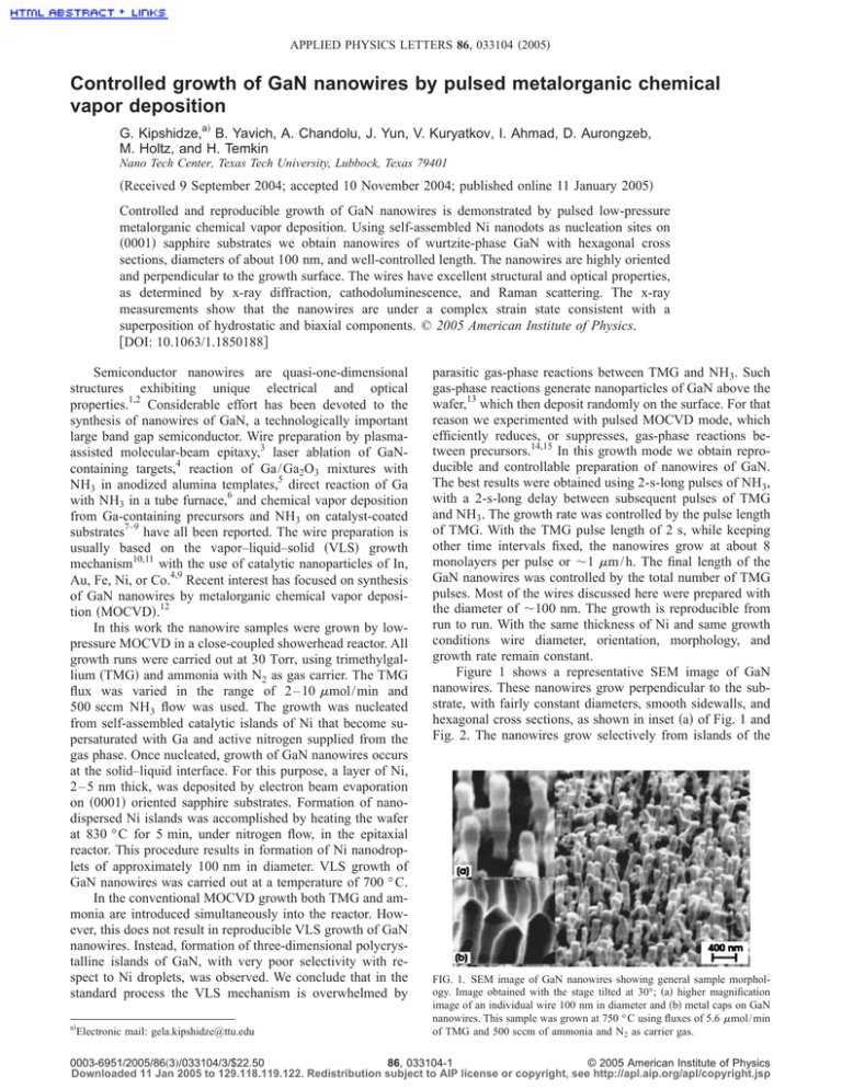
APPLIED PHYSICS LETTERS 86, 033104 共2005兲 Controlled growth of GaN nanowires by pulsed metalorganic chemical vapor deposition G. Kipshidze,a兲 B. Yavich, A. Chandolu, J. Yun, V. Kuryatkov, I. Ahmad, D. Aurongzeb, M. Holtz, and H. Temkin Nano Tech Center, Texas Tech University, Lubbock, Texas 79401 共Received 9 September 2004; accepted 10 November 2004; published online 11 January 2005兲 Controlled and reproducible growth of GaN nanowires is demonstrated by pulsed low-pressure metalorganic chemical vapor deposition. Using self-assembled Ni nanodots as nucleation sites on 共0001兲 sapphire substrates we obtain nanowires of wurtzite-phase GaN with hexagonal cross sections, diameters of about 100 nm, and well-controlled length. The nanowires are highly oriented and perpendicular to the growth surface. The wires have excellent structural and optical properties, as determined by x-ray diffraction, cathodoluminescence, and Raman scattering. The x-ray measurements show that the nanowires are under a complex strain state consistent with a superposition of hydrostatic and biaxial components. © 2005 American Institute of Physics. 关DOI: 10.1063/1.1850188兴 Semiconductor nanowires are quasi-one-dimensional structures exhibiting unique electrical and optical properties.1,2 Considerable effort has been devoted to the synthesis of nanowires of GaN, a technologically important large band gap semiconductor. Wire preparation by plasmaassisted molecular-beam epitaxy,3 laser ablation of GaNcontaining targets,4 reaction of Ga/ Ga2O3 mixtures with NH3 in anodized alumina templates,5 direct reaction of Ga with NH3 in a tube furnace,6 and chemical vapor deposition from Ga-containing precursors and NH3 on catalyst-coated substrates7–9 have all been reported. The wire preparation is usually based on the vapor–liquid–solid 共VLS兲 growth mechanism10,11 with the use of catalytic nanoparticles of In, Au, Fe, Ni, or Co.4,9 Recent interest has focused on synthesis of GaN nanowires by metalorganic chemical vapor deposition 共MOCVD兲.12 In this work the nanowire samples were grown by lowpressure MOCVD in a close-coupled showerhead reactor. All growth runs were carried out at 30 Torr, using trimethylgallium 共TMG兲 and ammonia with N2 as gas carrier. The TMG flux was varied in the range of 2 – 10 mol/ min and 500 sccm NH3 flow was used. The growth was nucleated from self-assembled catalytic islands of Ni that become supersaturated with Ga and active nitrogen supplied from the gas phase. Once nucleated, growth of GaN nanowires occurs at the solid–liquid interface. For this purpose, a layer of Ni, 2 – 5 nm thick, was deposited by electron beam evaporation on 共0001兲 oriented sapphire substrates. Formation of nanodispersed Ni islands was accomplished by heating the wafer at 830 ° C for 5 min, under nitrogen flow, in the epitaxial reactor. This procedure results in formation of Ni nanodroplets of approximately 100 nm in diameter. VLS growth of GaN nanowires was carried out at a temperature of 700 ° C. In the conventional MOCVD growth both TMG and ammonia are introduced simultaneously into the reactor. However, this does not result in reproducible VLS growth of GaN nanowires. Instead, formation of three-dimensional polycrystalline islands of GaN, with very poor selectivity with respect to Ni droplets, was observed. We conclude that in the standard process the VLS mechanism is overwhelmed by a兲 Electronic mail: gela.kipshidze@ttu.edu parasitic gas-phase reactions between TMG and NH3. Such gas-phase reactions generate nanoparticles of GaN above the wafer,13 which then deposit randomly on the surface. For that reason we experimented with pulsed MOCVD mode, which efficiently reduces, or suppresses, gas-phase reactions between precursors.14,15 In this growth mode we obtain reproducible and controllable preparation of nanowires of GaN. The best results were obtained using 2-s-long pulses of NH3, with a 2-s-long delay between subsequent pulses of TMG and NH3. The growth rate was controlled by the pulse length of TMG. With the TMG pulse length of 2 s, while keeping other time intervals fixed, the nanowires grow at about 8 monolayers per pulse or ⬃1 m / h. The final length of the GaN nanowires was controlled by the total number of TMG pulses. Most of the wires discussed here were prepared with the diameter of ⬃100 nm. The growth is reproducible from run to run. With the same thickness of Ni and same growth conditions wire diameter, orientation, morphology, and growth rate remain constant. Figure 1 shows a representative SEM image of GaN nanowires. These nanowires grow perpendicular to the substrate, with fairly constant diameters, smooth sidewalls, and hexagonal cross sections, as shown in inset 共a兲 of Fig. 1 and Fig. 2. The nanowires grow selectively from islands of the FIG. 1. SEM image of GaN nanowires showing general sample morphology. Image obtained with the stage tilted at 30°; 共a兲 higher magnification image of an individual wire 100 nm in diameter and 共b兲 metal caps on GaN nanowires. This sample was grown at 750 ° C using fluxes of 5.6 mol/ min of TMG and 500 sccm of ammonia and N2 as carrier gas. 0003-6951/2005/86共3兲/033104/3/$22.50 86, 033104-1 © 2005 American Institute of Physics Downloaded 11 Jan 2005 to 129.118.119.122. Redistribution subject to AIP license or copyright, see http://apl.aip.org/apl/copyright.jsp 033104-2 Appl. Phys. Lett. 86, 033104 共2005兲 Kipshidze et al. TABLE I. Stress parameters of GaN nanowires. Lattice parameter Strain 共⫻10−4兲 Stress 共GPa兲 Raman shift 共cm−1兲 Sample a 共Å兲 c 共Å兲 a c Hydrostatic Biaxial Meas. Calc. GaN reference L = 1.5 m L = 0.8 m 3.1892 3.1891 3.1897 5.1855 5.1895 5.1874 ¯ −0.3 1.6 ¯ 7.7 3.7 ¯ −0.30 −0.17 ¯ −0.24 −0.06 ¯ −0.7± 0.2 −0.8± 0.2 ¯ −0.48 −0.55 metal catalyst and no deposits of GaN could be seen between the wires. A slight increase in the diameter of the growing wire, visible in Fig. 1共a兲, may be indicative of sidewall growth. Characteristic metal caps at nanowires tips, shown in the inset 共b兲 of Fig. 1, confirm the VLS mechanism of their formation. The shape of the caps is typical of Ni nanodots formed in high temperature, 830 ° C, anneals. These caps are easily removed with a wet etch. Formation of wires with triangular cross sections12 was not observed. XRD measurements were carried out to elucidate crystal structure of GaN nanowires. Symmetric 2 − scans carried on a sample of ⬃1-m-long nanowires over a wide angular range show only the 共0002兲 and 共0004兲 diffraction peaks of hexagonal GaN at 34.56° and 72.917°, respectively. The data clearly confirms the c-axis growth orientation and hexagonal nature of the wires. Symmetric reciprocal space map obtained for the 共0002兲 reflection of hexagonal GaN shows that the nanowires are under uniform strain. Nanowires of GaN grown by pulsed epitaxy are sufficiently uniform, in both length and diameter, to measure the a and c lattice constants. These were obtained from the measurements of symmetric 共0002兲 and asymmetric 共112̄4兲 reflections. The resulting lattice constants are listed in Table I for selected samples with ⬃100-nm-diam wires of different lengths 共L兲, together with the lattice constants of relaxed GaN used as a reference. These measurements demonstrate the presence of strain in nanowires of GaN. Optical properties of GaN layers were characterized by CL measurements at room temperature. Samples were excited with an electron beam with the energy of 1 – 9 keV, at a current of 100 A, with the excitation power density between 1.0 and 4.5 W / cm2. The spectra, shown in Fig. 2, exhibit a single peak at 3.36 eV 共⬃369 nm兲 which we attribute to band-edge-related emission. This peak is redshifted, by ⬃70 meV, with respect the band edge of hexagonal GaN. The slight redshift can be attributed to strain in GaN nanowires, as discussed in the following. Deep level CL emission was not observed. The inset shows a high magnification SEM image of a single nanowire confirming its hexagonal symmetry. As seen in Table I both the a and c lattice constants of our GaN nanowires differ from those of the reference sample, indicating that the wires are strained. Uniform layers of GaN on sapphire are usually under compressive biaxial stress, resulting in a ⬍ 0 and c ⬎ 0. This is not the case of all nanowire samples studied here. In addition, the values of Poisson ratio evaluated from our measurements are not consistent with the expected value of 0.23± 0.06 for GaN under compressive biaxial strain.16 This suggests a more complex strain state, a combination of hydrostatic and biaxial strains according to = C, where is the stress tensor, C is the elastic compliance tensor,17 and is the associated strain tensor. In our analysis, we assume a diagonal strain tensor = 冤 a a c 冥 共1兲 with the associated stress tensor 冤 冥 冤 冥 1 =−P 1 + b 1 1 1 , 共2兲 0 where P is the effective hydrostatic pressure and b is the biaxial component of stress. This analysis allows us to determine both unknown components of the stress tensor from the two experimentally determined strains a and c. Results of Table I illustrate the range of stress values determined for GaN nanowires with different length. Externally applied hydrostatic pressure is always compressive. Hence, P ⬍ 0 indicates a tensile internal strain. Clearly, the hydrostatic component is significant. Such component is occasionally present in uniform layers of GaN and attributed to point defects.16,18,19 Following the approach of Ref. 16, it is possible to estimate the concentrations of likely point defects responsible for this internal strain. Nickel is a plausible candidate, since it is possible that small amounts are incorporated into the growing GaN nanowires forming Ni–Ga intermetallics. A straightforward calculation would suggest Ni concentrations as high as 0.1%. This high value seems unlikely, since we do not detect any Ni–Ga compounds in our wide angle x-ray diffraction measurements. In addition, high defect concentrations, which generally quench band-gap-related luminescence, are not consistent with the CL spectra of our samples. Internal strain driven by surface relaxation has been proposed recently to account for stiffening of nanoparticles.20 Inclusion of such a mechanism, unique to nanostructures, may be necessary to account for the strain measured in our nanowires. Biaxial stress in epitaxial GaN layers grown on sapphire stems from residual and thermal stresses. Values are typically on the order of −0.5 GPa.21 The maximum thermal stress calculated for ideal GaN layers grown on sapphire at 700 ° C is ⬃−1 GPa.22,23 In comparison, the biaxial stress term for our nanowires varies from negligibly small, −0.06 GPa in wires with the length of 0.8 m, to −0.24 GPa in 1.5-m-long wires. Thus, our short nanowires show almost complete relaxation. Based on the stress states determined from our x-ray measurements, we can also estimate the expected shift in the GaN energy gap for our nanowires. Using hydrostatic and uniaxial coefficients from Refs. 24 and 25 we estimate this Downloaded 11 Jan 2005 to 129.118.119.122. Redistribution subject to AIP license or copyright, see http://apl.aip.org/apl/copyright.jsp 033104-3 Appl. Phys. Lett. 86, 033104 共2005兲 Kipshidze et al. calculate the expected Raman shift of the E22 phonon. The experimental and calculated values of the Raman shift are shown in Table I. Good agreement seen in both sets of values supports our interpretation of the nanowires1 stress discussed earlier. In summary, we report reproducible growth of GaN nanowires by pulsed MOCVD from Ni nanodots. X-ray diffraction and optical measurements confirm the wurtzite structure, c-axis growth orientation, and excellent structural and optical properties. The stress state in the wires is interpreted as a combination of hydrostatic and biaxial, with good agreement obtained between x-ray and Raman measurements. FIG. 2. Room temperature cathodoluminescence spectrum of 100-nm-diam GaN nanowires grown by pulsed MOCVD. Inset shows a high magnification SEM image of a single hexagonal nanowire. redshift to be 30– 40 meV. This is in reasonable agreement with what we report above for our CL measurements, without taking into account further factors such as the Stokes shift and shallow defect states, each of which would produce a redshift. Additional information on the stress state of our nanowires is obtained using Raman spectroscopy. Figure 3 shows a representative room temperature Raman spectrum of the 0.8-m-long nanowire sample 共see Table I兲. The spectrum shows two lines—E22, which is symmetry allowed in backscattering along the wurtzite c axis, and a weak symmetry forbidden A1共TO兲. The latter is most likely seen due to right angle scattering occurring when the incident light enters the nanowires sidewalls, as illustrated in the inset of Fig. 3. The narrow linewidth of the E22 phonon, ⬃6 cm−1, is comparable to that obtained on high quality epitaxial GaN, confirming high crystal quality of the nanowires. The position of the strong E22 line is commonly used to determine stress in epitaxial GaN. Taking the stress values listed in Table I and known Raman shifts for hydrostatic pressure 共4.24 cm−1 / GPa兲26 and biaxial stress 共3.24 cm−1 / GPa兲22 we FIG. 3. Room temperature Raman spectra of GaN nanowires. The inset depicts the mechanism by which both backscattering and right angle scattering is possible, with incident 共scattered兲 wavelength denoted as L 共S兲. The authors acknowledge support for this research from the National Science Foundation 共ECS-0304224, ECS0210141 and ECS-0323640兲 and the J. F Maddox Foundation. 1 Y. Xia, P. Yang, Y. Sun, Y. Wu, B. Mayers, B. Gates, Y. Yin, F. Kim, and H. Yan, Adv. Mater. 共Weinheim, Ger.兲 15, 353 共2003兲. 2 Z. Zhong, F. Qian, D. Wang, and C. M. Lieber, Nano Lett. 3, 343 共2003兲. 3 V. V. Mamutin, Tech. Phys. Lett. 25, 741 共1999兲. 4 X. Duan and C. Lieber, J. Am. Chem. Soc. 122, 188 共2000兲. 5 G. Chen, L. Zhang, Y. Zhu, G. Fei, L. Li, C. Mo, and Y. Mao, Appl. Phys. Lett. 75, 2455 共1999兲. 6 M. He, P. Zhou, S. Noor Mohammad, G. L. Harris, J. B. Halpern, R. Jacobs, W. L. Sarney, and L. Salamanca-Riba, J. Cryst. Growth 231, 357 共2001兲. 7 S. Han, W. Jin, T. Tang, C. Li, D. Zhang, and X. Liu, J. Mater. Res. 18, 245 共2003兲. 8 T. Y. Kim, S. H. Lee, Y. H. Mo, H. W. Shim, K. S. Nahm, E.-K. Suh, J. W. Yang, K. Y. Lim, and G. S. Park, J. Cryst. Growth 257, 97 共2003兲. 9 G. Cheng, A. Kolmakov, Y. Zhang, M. Moskovits, R. Munden, M. Reed, G. Wang, D. Moses, and J. Zhang, Appl. Phys. Lett. 83, 1578 共2003兲. 10 R. S. Wagner and W. C. Ellis, Appl. Phys. Lett. 4, 89 共1964兲. 11 R. S. Wagner, W. C. Ellis, K. A. Jackson, and S. M. Arnold, J. Appl. Phys. 35, 2993 共1964兲. 12 T. Kuykendall, P. Pauzauskie, S. Lee, Y. Zhang, J. Goldberger, and P. Yang, Nano Lett. 3, 1063 共2003兲. 13 J. R. Creighton, W. G. Breiland, M. E. Coltrin, and R. P. Pawlowski, Appl. Phys. Lett. 81, 2626 共2002兲. 14 M. Asif Khan, R. A. Skogman, J. M. Van Hove, D. T. Olson, and J. N. Kuznia, Appl. Phys. Lett. 60, 1366 共1992兲. 15 J. Zhang, E. Kuokstis, Q. Fareed, H. Wang, J. Yang, G. Simin, M. Asif Khan, R. Gaska, and M. Shur, Appl. Phys. Lett. 79, 925 共2001兲. 16 C. Kisielowski, J. Krüger, S. Ruvimov, T. Suski, J. W. Ager III, E. Jones, Z. Liliental-Weber, M. Rubin, E. R. Weber, M. D. Bremser, and R. F. Davis, Phys. Rev. B 54, 17745 共1996兲. 17 A. F. Wright, J. Appl. Phys. 82, 2833 共1997兲. 18 M. Katsikini, K. Papagelis, E. C. Paloura, and S. Ves, J. Appl. Phys. 94, 4389 共2003兲. 19 M. J. Aziz, Appl. Phys. Lett. 70, 2811 共1997兲. 20 B. Gilbert, F. Huang, H. Zhang, G. A. Waychunas, and J. F. Banfield, Science 305, 651 共2004兲. 21 J. Keckes, J. W. Gerlach, R. Averbeck, H. Riechert, S. Bader, B. Hahn, H.-J. Lugauer, A. Lell, V. Harle, A. Wenzel, and B. Rauschenbch, Appl. Phys. Lett. 79, 4307 共2001兲. 22 I. Ahmad, M. Holtz, N. N. Faleev, and H. Temkin, J. Appl. Phys. 95, 1692 共2004兲. 23 H. Hiramatsu, T. Detchprohm, and I. Akasaki, Jpn. J. Appl. Phys., Part 1 32, L1528 共1993兲. 24 P. Perlin, I. Gorczyca, N. E. Christensen, I. Grzegory, H. Teisseyre, and T. Suski, Phys. Rev. B 45, 13307 共1992兲. 25 D. G. Zhao, S. J. Xu, M. H. Xie, S. Y. Tong, and H. Yang, Appl. Phys. Lett. 83, 677 共2003兲. 26 A. R. Goňi, H. Siegle, K. Syassen, C. Thomsen, and J.-M. Wagner, Phys. Rev. B 64, 035205 共2001兲. Downloaded 11 Jan 2005 to 129.118.119.122. Redistribution subject to AIP license or copyright, see http://apl.aip.org/apl/copyright.jsp
![Structural and electronic properties of GaN [001] nanowires by using](http://s3.studylib.net/store/data/007592263_2-097e6f635887ae5b303613d8f900ab21-300x300.png)
