unit-1 - WordPress.com
advertisement
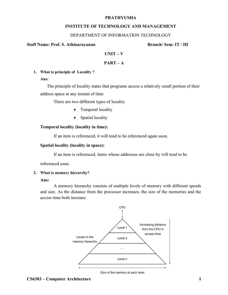
PRATHYUSHA INSTITUTE OF TECHNOLOGY AND MANAGEMENT DEPARTMENT OF INFORMATION TECHNOLOGY Staff Name: Prof. S. Athinarayanan Branch/ Sem: IT / III UNIT – V PART – A 1. What is principle of Locality ? Ans: The principle of locality states that programs access a relatively small portion of their address space at any instant of time There are two different types of locality Temporal locality Spatial locality Temporal locality (locality in time): If an item is referenced, it will tend to be referenced again soon. Spatial locality (locality in space): If an item is referenced, items whose addresses are close by will tend to be referenced soon. 2. What is memory hierarchy? Ans: A memory hierarchy consists of multiple levels of memory with different speeds and size. As the distance from the processor increases, the size of the memories and the access time both increase. CS6303 – Computer Architecture 1 3. Define cache hit rate and cache miss rate? Ans: Cache Hit Rate The fraction of memory access found in cache is called cache hit rate. It is often used as a measure of the performance of cache memory. Cache Miss Rate Cache Miss rate is the fraction of memory access not found in cache is called cache miss rate. Cache miss rate = 1- cache hit rate. 4. List four memory technologies used today in memory hierarchies? Ans: The four technologies used today in memory hierarchies are SRAM semi conductor memory DRAM semi conductor memory Flash semi conductor memory Magnetic disk 5. The disk rotate at 5400 rpm, find out the average rotational latency? Ans: Average rotational latency = 0.5 /5400 rpm = 0.5 /(5400 / 60) = 30/5400 = 0.0056 = 5.6 ms CS6303 – Computer Architecture 2 6. Draw the cell diagram of SRAM and DRAM? Ans: Bipolar Static RAM Asynchronous Dynamic RAM (DRAM) 7. Compare SRAM and DRAM? Ans: PARAMETER DYNAMIC RAM STATIC RAM 1. Cell Type Flip Flop Cell Capacitor Storage Cell 2. Speed Fast Slow 3. Refreshing Not Required Required 4. Density Less More 5. Cost More Less CS6303 – Computer Architecture 3 8. Define seek time and rotational latency of disk memory? Ans: Seek Time Time to move the head to the desire track is called seek time. Rotational latency The time required for desired sector of a disk to rotate under the read/write head, usually average rotational latency assumed to be half of the rotation time. 9. What is cache memory? Ans: A small, fast memory introduced between the processor and the main memory is called cache memory which improves the effective speed of the memory. 10. What is split cache? Ans: Split cache consist of two independent caches. That operate in parallel in each other, with one handling instruction and one handling data. 11. Write effective access time of cache memory? Ans: Effective access time of cache memory = cache access time x hit rate + (1- hit rate) x main memory access time. CS6303 – Computer Architecture 4 12. How 32 bit virtual address is divided if the page size is 16k bytes? Ans: Page size = 16K No. of address bits = 14 No. of bits for page numbers = 32 – 14 = 18 bits Page Number Page offset 18 14 13. Compare I/O mapped I/O and memory mapped I/O. Ans: Memory Mapped 1. I/O Mapped Part of memory space is used as Separate I/O Address space Intel I/O address Motorola – 6800 – 8085 2. No Separate I/O instruction Separate I/O Instruction (In / Out) 3. Extra decoding Logic No extra Logic 14. What is I/O interface and list its components? Ans: The hardware required to connect an Input / Output device to the bus is called I/O interface The major components of I/O interface are i. Address decoder ii. Control circuit iii. Data & status register 15. What is interrupt and interrupt service routine? Ans: In response to an event (external or internal) the CPU transfer the control from its current program to another program an interrupt handler (Interrupt Service Routine) that services the event Interrupt Service Routine (ISR) is a small program which takes appropriate actions for the event. CS6303 – Computer Architecture 5 16. What is vectored interrupt? Ans: Here an interrupt request from a device causes a direct transition to the correct ISR. For this device must supply the CPU with the starting address of interrupt vector of the program. 17. What is DMA? Ans: In a programmed I/O each character is transferred from I/O to processor register under CPU control. However in DMA, the block of data is directly transferred between external device and memory without involving CPU. This type of I/O is called DMA. 18. What is IOP? Ans: IOP stands for Input Output Processor. Like CPU, IOP is a processor with restricted (simple) instruction set, mainly used to take care I/O operation. Hence the powerful processor is relieved from this simple work. This is also called peripheral processing unit. 19. What is Bus? How the bus lines are grouped? Ans: The components of a computer system CPU, Memory and I/O Units are connected by a group of wires called Bus The system bus consists of 3 group of lines a. Address b. Data and c. Control CS6303 – Computer Architecture 6 20. Find the AMAT for a processor with 1 ns clock cycle time and miss penalty of 20 cycles, a miss rate of .05 miss per instruction and a cache access time including hit detection of 1 clock cycle. Assume read 7 write miss penalty are the same and ignore other write state. Ans: The average memory access time is AMAT = hit rate X cache cycle time + miss rate X miss penalty = .95 X 1 + .05 (20) = 1.95 n sec CS6303 – Computer Architecture 7 PART – B 1. Explain direct mapped cache memory with suitable diagram? Ans: A small, fast memory introduced between the processor and the main memory is called cache memory which improves the effective speed of the memory. Use of a Cache Memory CACHE MAPPING ALGORITHM The correspondence between the main memory and cache is specified by MAPPING FUNCTION The Popular mapping functions are a. Direct mapping b. Associative mapping c. Set associative mapping Direct Mapped Cache CS6303 – Computer Architecture 8 a. DIRECT MAPPING This is explained by taking a specific example Consider a cache consisting of 128 blocks of 16 words for a total of 2048 words and assume that the main memory is 64K words Both main memory and cache memory is divided into blocks of size equal to 16 words Here block j of main memory maps to (block j mod 128) of cache. Main memory blocks 0, 128, 256 … loaded into cache block 0 Main memory blocks 1, 129, 257 … loaded into cache block 1 and so on Placement of a block in the cache is determined from memory address Memory address is divided into three fields as shown in figure Lower order 4 bit select one of 16 words within a block Next 7 bits select cache block Next 5 bit decides block from which segment is mapped to cache. During processing higher order 5 bits are compared with tag bits of cache block pointed by 7 bit cache block field If match – desired word is in the block – Cache Hit If not – desired word is brought from main memory and loaded to cache – Cache Miss Advantages: It is easy to implement. Disadvantages: Contention CS6303 – Computer Architecture 9 2. Explain virtual memory implementation with address translation? Ans: In a Computer system (without virtual storage) the program size is limited by the physical memory available in the system. However the virtual memory system extends the apparent size of the physical memory equal to the address space of the processor. The address translation from the virtual address to the physical address is carried out by a unit called Memory Management Unit (MMU) as shown in diagram below. Virtual Memory Organisation CS6303 – Computer Architecture 10 ADDRESS TRANSLATION The address translation is shown in figure below. Virtual Memory Address Translation Programs and data composed of fixed length unit called PAGES Page table is used to keep address of main memory location for each page and its status the page table kept in the main memory Page Table Base Register: Starting address of page table is stored in this register To get the page table entry for a virtual address, the virtual page number is added to the content of page table base register. The page table entry gives the physical page number. This physical page number to which virtual address offset is added to give the physical address of main memory When the processor generates a virtual address the page table entry confirms that the page is not available in memory is called PAGE FAULT. To Speedup the Address Translation CS6303 – Computer Architecture 11 Every time the CPU generate virtual address; MMU has to translate the virtual address to physical address, for this page table entry corresponding to virtual address page has to be read from page table. Use of an associative mapped TLB To avoid this access time and degradation of performance, recently translated virtual page and its corresponding physical page is kept in a buffer and this buffer is called Translation Look aside Buffer (TLB) When a processor i.e. MMU finds the page table entries in TLB, it does not have to access the page table and saves substantial access time. CS6303 – Computer Architecture 12 3. Explain I/O and memory mapped I/O. Ans: The components of a computer system CPU, Memory and I/O Units are connected by a group of wires called Bus The system bus consists of 3 group of lines a. Address b. Data and c. Control Methods of I/O Addressing There are two methods of I/O addressing a. I/O mapped I/O b. Memory mapped I/O a. I/O mapped I/O - Here the processor has separate I/O and memory space - The memory reference instruction activates Read M or Write M control line which will not affect I/O device - The CPU has separate Input / Output instruction which activates Read I/O or Write I/O - This method is used in intel 8085 I/O Mapped I/O CS6303 – Computer Architecture 13 b. Memory mapped I/O - Here there is no separate I/O address and no I/O instructions - Here some memory address is reserved for I/O register by the designer - This method is used in Motorola - 6800 Memory Mapped I/O Comparison of I/O Mapped I/O and Memory Mapped I/O Memory Mapped I/O I/O Mapped I/O Part of memory space is used as I/O address Separate I/O Address space Intel – Motorola – 6800 8085 2. No Separate I/O instruction Separate I/O Instruction (In / Out) 3. Extra decoding Logic No extra Logic 1. CS6303 – Computer Architecture 14 4. Briefly explain I/O interface and its components. Ans: The hardware required to connect an Input / Output device to the bus is called I/O interface The major components of I/O interface are i. Address decoder ii. Control circuit iii. Data & status register Address Decoder: Enables the device to recognize its address when this address appears on the address lines. Data Register: This holds the data being transferred to or appears on the data lines. Status Register: Contains information relevant to the operation of the I/O device. CS6303 – Computer Architecture 15 5. Explain how a character is moved from a keyboard to processor using programmed I/O method. Ans: The connection between keyboard and the processor is shown below Bus Processor DATAIN SIN Keyboard Bus connections between processor and keyboard Striking a character stores the corresponding character in Data in (8 bit Buffer Register) The availability of character is indicated by a Flag SIN (Status Control Flag) The processor checks this flag and if the flag is set, the processor will read the character from data in Readwait: BR Readwait if SIN = 0 IN Datain, R1 Reading the character from datain to register, will clear sin flag This procedure repeats for each character CS6303 – Computer Architecture 16 6. Explain the different type’s interrupts of a processor. Ans: Interrupt Hardware are classified as 1. Single Line interrupt 2. Multiline Interrupt 1. Single Line Interrupt - Here a single interrupt line is used to serve n devices. - All the devices are connected to the line via switch to ground - INTR is logical OR of the requests from individual devices. INTR = INTR1 + INTR2 + …. + INTRN Single Line Interrupt 2. Multiline Interrupt - Here each I/O unit request Interrupt on a separate line and each one is assigned a separate priority - The source of interrupt is known to the CPU thus eliminating the scan of I/O ports. - Here also the CPU has to execute a program to fetch the address of ISR and this step can be eliminated in VECTORED INTERRUPT CS6303 – Computer Architecture 17 Multiline Interrupt 3. Vectored Interrupt - Here an interrupt request from a device caused a direct transition to the correct ISR - For this the device must supply the CPU with the starting address or interrupt vector of the program Vectored Interrupt Enabling / Disabling Interrupts - Interrupts request are stored on Interrupt Registers - Interrupt MASK REGISTER can disable any or all the interrupt under program control - By setting bit i of mask register to 1 interrupt request line i is disabled and by setting bit i of mask register to 0 interrupt request line i is enabled (a) System with vectored Interrupt CS6303 – Computer Architecture (b)Location of ISRs 18 7. Explain the operation of DMA with the circuit diagram. Ans: In a programmed I/O each character is transferred from I/O to processor register under CPU control. However in DMA, the block of data is directly transferred between external device and memory without involving CPU. This type of I/O is called DMA. The circuit which performs DMA is called DMA controller. Circuit required for DMA DMA Data Transfer 1. CPU Load the counter and address Reg with initial values Counter – contain the number of words to be transferred Address Reg – contain the starting address of the block to be transferred 2. When DMA Controller is ready to transmit or receive It activates DMA request to CPU CPU waits for the next DMA Breakpoint and activate DMA acknowledge CS6303 – Computer Architecture 19 DMA request & DMA acknowledge are essentially bus request and bus grant lines 3. The DMA controller now transfers data directly to or from memory. After each word is transferred Address Register, Word Counter is updated. 4. The Step 3 is repeated until word counter reaches Zero. DMA controller now give back the controls of the system bus it may also send the interrupt signal to CPU. The CPU responds by halting the I/O device or by initiating another DMA transfer. DMA & Interrupt Break Points - Interrupt can take place – between two instruction - DMA interrupt can take place every bus cycle of the instruction Types of data Transfers in DMA a) DMA Block Transfer: Block of words is transferred in a single burst, while DMA controller is the master of Bus b) Cycle Stealing: This allows the DMA controller to use the system bus to transfer one data word and return the control to CPU. Hence long block of I/O data are transferred by a sequence of DMA transactions interspersed with CPU transactions. CS6303 – Computer Architecture 20 8. Short note on I/O processor. Ans: IOP stands for Input Output Processor. Like CPU, IOP is a processor with restricted (simple) instruction set, mainly used to take care I/O operation. Hence the powerful processor is relieved from this simple work. This is also called Peripheral Processing Unit. IOP Works in Parallel to CPU IOP is referred as Channels in IBM system / 360 I/O Instructions The figure shows I/O instructions in IBM system 360 series and its successors where IOPs are preferred as channels Format of I/O Instructions The CPU Instructions has OPCODE & Address of field which give IOP Numbers and I/O Address There are three major instructions of the Type START I/O - To Initiate I/O HALT I/O - To Terminate I/O TEST I/O - To check the status bits of I/O The Instruction executed by IOP are called Channel Commands Words and the format is shown in figure. They are three types Data Transfer Instruction CS6303 – Computer Architecture – Includes Read & Write 21 Branch Instruction – This permit to fetch next CCW from specified memory location I/O Device Instruction – These are sent to I/O device and specify function to be performed in that device System Organization computer having IOP IOP, CPU share access to a common memory via system bus Memory stores separate program for CPU & IOP This also contain communication area for communication between two processors CPU alert IOP attention by START I/O The IOP get CPU attention by Interrupt The figure give interaction between IOP & CPU CS6303 – Computer Architecture 22
