ELE3103 Applied Analogue Electronics
advertisement
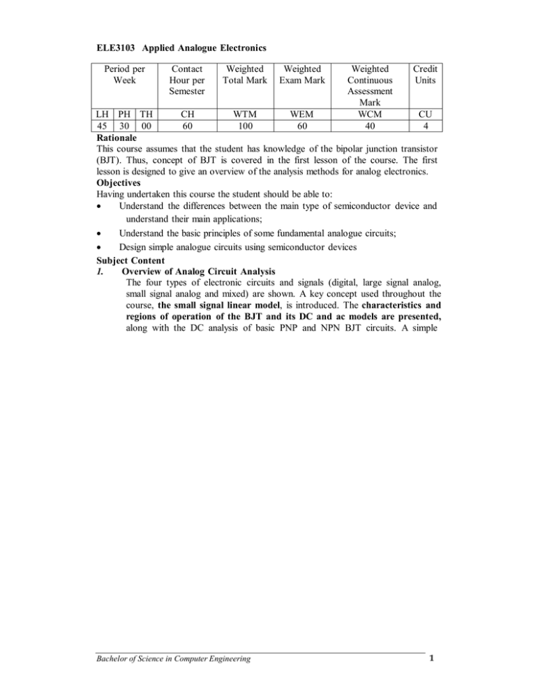
ELE3103 Applied Analogue Electronics Period per Week Contact Hour per Semester Weighted Total Mark Weighted Exam Mark Weighted Continuous Assessment Mark WCM 40 Credit Units LH PH TH CH WTM WEM CU 45 30 00 60 100 60 4 Rationale This course assumes that the student has knowledge of the bipolar junction transistor (BJT). Thus, concept of BJT is covered in the first lesson of the course. The first lesson is designed to give an overview of the analysis methods for analog electronics. Objectives Having undertaken this course the student should be able to: Understand the differences between the main type of semiconductor device and understand their main applications; Understand the basic principles of some fundamental analogue circuits; Design simple analogue circuits using semiconductor devices Subject Content 1. Overview of Analog Circuit Analysis The four types of electronic circuits and signals (digital, large signal analog, small signal analog and mixed) are shown. A key concept used throughout the course, the small signal linear model, is introduced. The characteristics and regions of operation of the BJT and its DC and ac models are presented, along with the DC analysis of basic PNP and NPN BJT circuits. A simple Bachelor of Science in Computer Engineering 1 2. 3. 4. amplifier circuit is used to emphasize: a) the use of the small signal model to find the gain and phase relationship of the output to the input signal; b) superposition of small ac signals with DC bias voltage; and c) coupling capacitors used for isolation of the signal source from DC biasing. Using the general model of a small signal amplifier, the effect of the signal source internal resistance and load resistances on the overall gain of amplifier circuits is shown. A review of basic circuit analysis techniques including current division, voltage division, potential difference, node analysis and current and voltage sources from the point of view of I/V characteristics is given if necessary. Concepts of Input and Output Impedance, and Voltage Gain and Phase for Single-stage Amplifiers. The five basic equations for the impedance looking into the 3 terminals of BJT and MOSFET transistors, replaced by their small signal models, are derived using the vIN/iIN method. The six basic transistor circuit configurations (common source CS, common gate CG, and common drain CD for FET circuits; common emitter CE, common collector CC, and common base CB for BJT circuits) are introduced. DC and Small Signal Analysis of CE, CC, and CB Single Stage BJT Amplifiers. The DC bias or quiescent point (Q-Point) analysis for a BJT amplifier is reviewed and practiced. The impedance results from the v IN/i IN method are used to find the input impedance, output impedance, and signal gain of the three different types of BJT amplifiers (CE, CC and CB) using the impedance equations derived in lesson 2. The "input impedance" analysis method for a single stage CE BJT amplifier is compared with the classical "plug-in model" method. The basic concepts learned in lessons one and two are practiced and reinforced by finding the voltage gain of single stage amplifiers. A graphical presentation of how signal distortion is related to the Q point location is presented. DC and Small Signal Analysis of FET Amplifiers. The methods for finding the voltage gain and input and output impedance for the CS, CD, and CG FET amplifiers are presented. Emphasis is placed on using impedance concepts to find the voltage gain as well as the input and output impedance of amplifiers, without drawing the circuit models. The principles for setting the DC Q-point of an FET amplifier to meet small signal voltage gain specs are illustrated by a design example. The principles of the previous lessons are exercised by solving FET and BJT single stage amplifier problems. 5. Review of the Single Stage BJT Amplifiers; Design of Single Stage BJT and FET Differential Amplifiers with Low Output Impedance and High Input Impedance. The basic single stage differential amplifier, with emphasis on its discrimination against external noise, is introduced. The principles for the differential mode (DM) and common mode (CM) signal analysis of both BJT and FET differential amplifiers are presented. The origin of internal noise due to the random motion of charge in electronic circuits is presented, including basic concepts as Johnson, shot and flicker noise, dependence on the bandwidth, and signal to noise power ratio (SNR) equations are introduced. Bachelor of Science in Computer Engineering 2 6. Differential and Common Mode Analysis of Multistage Differential Amplifiers and the Common Mode Rejection Ratio. The virtual ground concept for the differential principles for analysis of multistage amplifiers emphasized. DC and small signal analyses differential amplifiers with current source bias source circuits are introduced 7. mode analysis is derived. The using impedance concepts are methods for FET and BJT are studied. Basic DC current Design of Current Sources and Three-stage CMOS Differential Amplifiers with Active P-channel Loads. Basic current mirror circuits in integrated circuit (IC) amplifiers are studied further from both DC and small signal view-of-points. Small signal analyses of classical multi-transistor current sources are done to review the method of finding output impedance and to show that these circuits can increase the output resistance and also improve the R OUTIOUT figure of merit for current sources. The method of suppressing common mode gain in CMOS Differential Amplifiers using P-channel current mirror loads is studied. Finding the voltage gain of three stage CMOS Differential Amplifiers by inspection is practiced. 8. Low and High Frequency Analysis of Single and Multistage Amplifiers. The fundamentals of the frequency and time response of RC circuits and Bode phase and gain plots, including the mathematics background, are reviewed. The short circuit time constant (SCTC) method for obtaining the low cutoff frequency of amplifiers is explained. Circuit problems exercising this method for the different configurations of single-stage amplifiers are solved. The high frequency models for the FET and BJT are presented along with gainbandwidth limitations. The high frequency response of common base, common gate, common collector, and common drain amplifiers (obtained by the open circuit time constant (OCTC) method) are compared. The Miller effect is derived and applied to the frequency response analysis of basic amplifier circuits. 9. Analysis and Design of Multi-stage BJT and FET Circuits with Feedback Circuits with feedback to improve input and output impedance, noise suppression, frequency response, gain stability, and nonlinear distortion are studied, along with methods to find the loop gain are studied. The classical feedback theory using amplifier and feedback “boxes” is briefly discussed. The frequency response of common base, common gate, common collector, and common drain amplifiers are compared. The tradeoffs between frequency response, gain, and input impedance and other parameters are emphasized. 10. Small Signal Parameters and Methods for Large Signal Analysis The concept of small signal parameters (z, y, h, and g) for analysis of two port electronic systems with the different feedback configurations (series-series, shunt-series, shunt-shunt, and series-shunt) is presented. The essential concepts and applications of two-port parameters for feedback systems and device characterization are listed. The graphical approach for large signal analysis of electronic circuits, as illustrated by analysis of the push-pull output stage of operational amplifier, is studied. There is at least one hour allocated to review for the final exam Bachelor of Science in Computer Engineering 3 Recommended and Reference Books [1] [2] R. C. Jaeger, Microelectronic Circuit Design, McGraw-Hill, New York, 1996; A. S. Sedra and K. C. Smith, Microelectronic Circuits, Oxford University Press, New York, 1998 Bachelor of Science in Computer Engineering 4
