EE122 - San Jose State University
advertisement
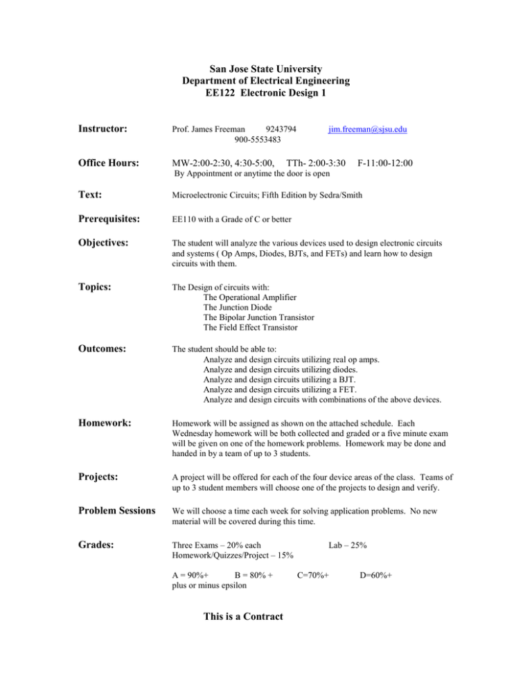
San Jose State University Department of Electrical Engineering EE122 Electronic Design 1 Instructor: Prof. James Freeman 9243794 900-5553483 Office Hours: MW-2:00-2:30, 4:30-5:00, jim.freeman@sjsu.edu TTh- 2:00-3:30 F-11:00-12:00 By Appointment or anytime the door is open Text: Microelectronic Circuits; Fifth Edition by Sedra/Smith Prerequisites: EE110 with a Grade of C or better Objectives: The student will analyze the various devices used to design electronic circuits and systems ( Op Amps, Diodes, BJTs, and FETs) and learn how to design circuits with them. Topics: The Design of circuits with: The Operational Amplifier The Junction Diode The Bipolar Junction Transistor The Field Effect Transistor Outcomes: The student should be able to: Analyze and design circuits utilizing real op amps. Analyze and design circuits utilizing diodes. Analyze and design circuits utilizing a BJT. Analyze and design circuits utilizing a FET. Analyze and design circuits with combinations of the above devices. Homework: Homework will be assigned as shown on the attached schedule. Each Wednesday homework will be both collected and graded or a five minute exam will be given on one of the homework problems. Homework may be done and handed in by a team of up to 3 students. Projects: A project will be offered for each of the four device areas of the class. Teams of up to 3 student members will choose one of the projects to design and verify. Problem Sessions We will choose a time each week for solving application problems. No new material will be covered during this time. Grades: Three Exams – 20% each Homework/Quizzes/Project – 15% A = 90%+ B = 80% + plus or minus epsilon This is a Contract Lab – 25% C=70%+ D=60%+ Date Topics 26-Jan 28-Jan 2-Feb 4-Feb 9-Feb 11-Feb 16-Feb 18-Feb Chapter 1- Linearity, Amplifiers, RC Time Constants Frequency Response, Bode Plots Chapter 2 - Operational Amplifiers CMRR, Slew rate, Stability Circuit Examples Circuit Examples Circuit Examples Circuit Examples 23-Feb 25-Feb 2-Mar 4-Mar 9-Mar Chapter 3 - Diodes Ideal Diode, Diode Types Half & Full Waver Rectification 11-Mar Chapter 4 - MOS Transistors 16-Mar 18-Mar 30-Mar 1-Apr 6-Apr 8-Apr 13-Apr 15-Apr 20-Apr 22-Apr 27-Apr 29-Apr 4-May 6-May 11-May 13-May BJT & MOS Device Characteristics Device Characteristics Device Switching CMOS Circuits DC Biasing Homework Projects 1 - 51, 53, 55, 68, 72, 77 2 - 20, 22, 50, 67, 71 72, 119, 126 Application Note 3 - 2, 3, 4, 10, 82, 91, 92 Op Amp Project Exam on Op Amps Limiting & Clamping Circuits 4 - 18, 19, 20, 30, 33, 35 4 - 42, 43, 61, 74, 75 78 4 - 88, 99, 101, Diode Project 10 - 14, 25, 29, 31 Exam on Diodes and CMOS MOS Amplifier Circuits MOS Amplifier Circuits MOS Amplifier Circuits Chapter 5 - BJTs Characteristics DC Biasing Single Stage Amplifiers Single Stage Amplifiers Single Stage Amplifiers Review Final This is an Estimate 5 - 48,56,57,75, MOS Project
