Chap3
advertisement
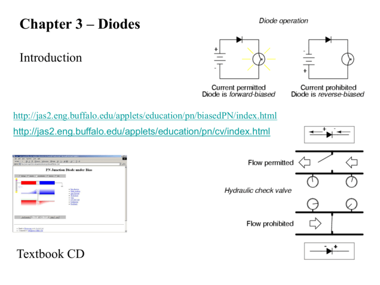
Chapter 3 – Diodes Introduction http://jas2.eng.buffalo.edu/applets/education/pn/biasedPN/index.html http://jas2.eng.buffalo.edu/applets/education/pn/cv/index.html Textbook CD Introduction The Ideal Diode The ideal diode: (a) diode circuit symbol; (b) i-v characteristic; (c) equivalent circuit in the reverse direction; (d) equivalent circuit in the forward direction. Rectifier Circuit Input waveform. Rectifier circuit Equivalent circuit when v1 > 0 Equivalent circuit when v1 0 Output waveform. Rectifier Circuit Example 3.1 Rectifier Circuit Example 3.2 Terminal Characteristics of Junction Diodes – Forward Region Example 3.3 Terminal Characteristics of Junction Diodes – Reverse-Bias Region Exercise 3.9 Rectifier Circuit Exercises 3.4 and 3.5 Diode – i-v Characteristic The i-v characteristic of a silicon junction diode. Diode – i-v Characteristic v n VT IS e 1 i VT k T Thermal Voltage q 25mV at room temp. for i>> Is i v v n VT IS e n VT ln IS i e is the base for the natural log The diode i-v relationship with some scales expanded and others compressed in order to reveal details. ln = 2.3 log Diode – i-v Characteristic Exercise 3.6 Consider a silicon diode with n=1.5. Find the change in voltage if current changes from 0.1 mA to 10 mA. v i IS e n VT v1 I1 IS e n 1.5 I1 0.0001 n VT v2 IS e n VT I2 0.01 ( v1 v2) I1 I2 VT 0.025 I2 e n VT v1_v2 n VT ln I1 I2 v1_v2 0.173 V Diode – i-v Characteristic A diode for which the forward voltage drop is 0.7 V at 1 mA and for which n=1 is operated at 0.5 V. What is the value of the current? v i IS e n VT 0.7 0.001 IS e 1 0.025 0.5 I IS e 1 0.025 0.2 I 0.001 e I 0.335 0.025 uA 6 10 Diode – Simplified Physical Structure Simplified physical structure of the junction diode. (Actual geometries are given on Appendix A.) Diode – Semiconductor Physics The semiconductor diode is what is called a pn junction and is shown in the figure on the right Both the p and the n sections are part of the same crystal of silicon. At room temp., some of the covalent bonds in silicon break and electrons are attracted to other atoms. These moving electrons leave a hole behind that is filled by another electron, thus continuing the cycle. In thermal equilibrium the concentration of holes (p) and the concentration of free electrons (n) are equal to each other and to ni which is the number of holes or free electrons in silicon at a given temp. Study of semiconductor physics yields the following equation for the free electrons. In this eqaution, B is a material dependant parameter (5.4x10^31) for silicon, E g is a parameter known as the bandgap energy (1.12electron volts (eV) for silicon), and k is the Boltsmann's constant (8.62x10^-5 eV/K). Thus, at room temp (300K), the number of holes or free electrons is 1.5x10^22. Diode – Semiconductor Physics The two methods by which holes and electrons move are called diffusion and drift. In diffusion, the flow moves from areas of higher concentration of p or n to areas of lower concentration. This flow gives rise to a flow of charge or diffusion current. This is given by the following Here, Jp is the current density (in Amps/cm^2), q is the magnitude of electron charge (1.6x10^-19C) and Dp is called the diffusivity of the holes. the differential dP is the rate of change for hole concentration. Jp d q D p P dx Jn Here, Jn is also the current density. The only difference is the differential dn. d q D n n Here, it stands for the rate of change of free electron concentration. dx Diode – Semiconductor Physics The other method is called drift. Free holes and e- are moved by an electric field (E) and have a velocity pE v drift p is the mobility of holes and has the units of (cm^2)/V*s. This method also gives rise to diffusion currents. q p p E Jp_drift Jn_drift q n n E The total drift current is written as follows. Jdrift q pp nn E Diode – Semiconductor Physics A relationship, known as the Einstein relationship can be noted below. Dn Dp n p The Vt term is what is called the thermal voltage. At room temperature, the thermal voltage is approximately equal to 25mV VT Silicon is often doped to give it better conductivity. Doping is the process by which impurity atoms are added to the silicon to provide more holes (p-type) or more free electrons (n-type). One thing to note is the way the various terms are defined. For n-type silicon, the hole concentration is n p and the electron concentration is nn . The concentration of donor (n-type) atoms or accpetor (p-type) atoms is denoted N d and NA respectively. Study of doped silicon revealed the following. 2 Pn ni ND nn Nd pp NA 2 np ni NA Diode – Semiconductor Physics The pn junction under open-circuit conditions When a diode (like the one shown above) is existing in a open circuit form two currents will naturally occur. Because the concentration of holes is high in the p-region and low in the n-region, holes will diffuse from the p-region to the n-region. Likewise, free electrons will diffuse from the n-region to the p-region. These two components add together to form the diffusion current Id whose direction is from the p-side to the n-side. When the free electrons diffuse to the p-side, many are paired up with holes very close to the border of the two regions thus depleting the number of free electrons. This uncovers a positive charge at the edge of the n-region. On the other side, due to the same (but exact opposite) situation, a negative charge is uncovered at the boundary of the p-region. This results in what is called the carrier-depletion region (shown in the figure below) because the two extremes create a potential difference to result. This is in the form of a barrier that holes and electrons must cross in order to create a current. Thus, it can be seen that the current ID depends on this barrier voltage (which is denoted V 0 ). Diode – Semiconductor Physics The voltage across this region can be found by the following equation: Vo NA ND VT ni2 In this equation, Na, Nd, and Vt are the same as they are previously defined above. In open circuit conditions, V0 is 0 because the voltages existing at the metal contacts of the diode (in the diagram above) counteract the voltage at the barrier. If this were not so, energy could be drawn from the isolated diode which is clearly incorrect. In addition to the diffusion current, there is also a drift current. When some of the thermally generated holes (holes created by a temp. increase which releases some outer electrons from their bonds) reach the edge of the depletion region, they are swept accross the area because of the electric field present in that region. This also happens to the free electrons. The addition of these two currents is the drift current Is which flows in the opposite direction of ID. Under open circuit conditions, no external current exists and the two currents are equal to each other. Under these conditions, if one current for some reason is not equal to the other, they will shift and change until the equilibrium is once again attained. Diode – Semiconductor Physics The carrier depletion region has a width and if the doping was equal for both the n and p regions, the depletion region would be symetrical. However, this is not the case so the widths will be different on either side. Because the depletion region has a balanced amount of charge, it will have to extend deeper into the lighter doped region so that the holes and electrons will all have a match. If the width in the p side is denoted x p and the width in the n side is x n , the charge-eqaulity condition is this: q xp A NA xn NA xp ND q xn A ND Here, A is the cross-sectional area of the junction. This equation can be rewritten to yield the following, more clear equality. In actual practice, one side is usually more heavily doped than the other causing the depletion region to exist almost entirely on one side (the lightly doped side). The width of the depletion region can be given (based on the above assumption that it exists mainly on one side) by the following equation. W depletion_region xn xp 1 1 V o q NA ND 2s In this equation, s is the electrical permittivity of silicon (1.04x10^-12 Farrads/cm). The width of the region is usually 0.1 to 1 m. Diode –Physical Structure The pn Junction under reverse-bias conditions To best describe the pn junction diode under reverse bias conditions, the diode is modelled to have a current source exciting it. This current is kept lower than I s to keep the diode from experiencing breakdown. The current (I) will be carried by electrons that move (in the opposite direction of I) from the n-region to the p-region. This process creates a voltage (denoted V r) for which the voltage tries to flow into the n-region of the diode. This voltage is, like the current, less than the breakdown voltage (the voltage at which current will flow in the negative direction). Because the positive end of the voltage is trying to enter the diode through the positive wall of the barrier, the voltage actually increases the barrier's size. No current, therefore, is allowed to pass through the diode. From this reasoning, it is relatively easy to see that as the current (and thus Vr) changes, the charge in the depletion region is going to change. In this way, the diode has some capacitance. The charge in the depletion region q j can be found by finding the charge in either of the two regions (because the charge is equal in both). Using the n-side, the following equation is derived. qj qn qj q q ND xn A NA ND NA ND For this equation, A is the cross-sectional area of the junction. Using the above eq. for the width of the depletion region, the following can be written A W depletion_region Here, Wdep is slightly different from the above equation and can be written as follows. Diode –Physical Structure 2s 1 1 This adjustment is made W depletion_region xn xpbecause Vo VR ND it is no longer an open circuit. q NA There is now an external voltage source acting on the diode so the voltage is the addition of the open circuit voltage and the reverse voltage. The capacitance can then be written as the derivative of the charge in the depletion region. WIth a little bit of algebra and the combining of previous equations, the value for the capacitance (C j ) can be found to be as follows: Cj0 Cj VR 1 V o Cj0 A m Here, Cjo is the value of the capacitance of the open circuit diode and is defined below. m is a value that depends on the manner in which the concentration changes from the p to the n side of the juncion. It is called the grading coefficient (for the case of the diode we are using, it is .5 but it ranges from .5 to about .333) q s NA ND 1 This is the value of the open circuit capacitance. This is 2 NA ND Vo readily made apparant by the fact that it does not depend on Vr. Diode –Physical Structure The pn Junction in the Breakdown Region As was explained earlier, the voltage for reverse bias conditions cannot exceed the breakdown voltage. If it does, the barrier will no longer hinder the flow of current. As the voltage, in reverse, accross the diode increases, the voltage across the depletion layer also increases. When this voltage is sufficiently high enough, one of two mechanisms comes into play that allows current to flow through the diode. The first of these mechanisms is called the zener effect. If the breakdown voltage of the diode is less than 5V, the zener effect is usually what happens. Zener breakdown occurs when the electric field in the depletion layer increases to the point where it can break covalent bonds and generate electron-hole pairs. These holes and pairs are then swept to their respective sides causing a reverse current to form which supports the outside current source. While this happens, the voltage across the diode will remain relatively close to the breakdown voltage while the current will be largely determined by the outside source. The other mechanism is called the avalanche effect. This usually happens when the breakdown voltage is greater than 7V. In this effect, the voltage or current basically forces its way through the barrier. The covalent bonds are broken by the incoming voltage/current and as the first few bonds break, more carriers are freed up to break more bonds causing an avalanche of current to flow. This causes large current changes for small voltage changes. A couple of things to note: 1. In the 5V to 7V range, the breakdown could be either zener or avalanche or a combination fo the two. 2. pn junction breakdown is not a destructive process. It only causes problems when the maximum dissapated power is exceeded. This max. value, in turn, implies a max. value for the reverse current. Diode –Physical Structure The pn Junction Under Forward-Bias Conditions When a diode is under forward bias condtions, an external voltage or current source is applied with the positive side of the voltage entering the p-side of the diode. When this happens, the electrons from the incoming current (which enter at the n-side) and the holes from the positive voltage (entering from the p-side) will nuetralize and diminish the depletion region barrier. A result of this is that the concentration of minority carriers at the edge of the depletion region (denoted pn(xn) is related to the forward voltage V by the following equation. V p n xn p n0 e VT In this equation, pn0 is the concentration of minority carriers when no external source is added. VT is the thermal voltage (ususlly 25mV). This is known as the law of the junction. The concentration of excess holes in the n-region can be expressed as the following. x xn p n( x) p n0 p n xn p n0 e Lp Here, Lp is a canstant that determines the steepness of the exponential decay of excess holes. It is called the diffusion length of holes in the n-type silicon. The smaller the value of Lp, the faster the injected holes will recombined with the majority electrons. The constant Lp is also related to another parameter called the excess-minority-carrier lifetime p. This is the average time it takes for an injected hole to recombine. Lp is also related to the diffusion constant Dp. Lp Dp p Typical values for Lp range from 1 to 100um and p usually ranges from 1 to 10,000ns. Diode –Physical Structure The holes diffusing in the n-region will give rise to a holes current. The density (which is greatest at the edge of the depletion region - x = xn) is given by the following. Jp V 1 VT Dp q p n0 e Lp In a similar manner, the analysis can extendd to the electrons injected into the p-region Jn V 1 VT Dn q n p0 e Ln is the diffusion length of the electrons in the p-region. Ln Because both of the densities are in the same direction, the total current (I) can be found. Substituting for pn0 = ni^2/ND and similarly for np0, the current can be expressed as follows. V 1 Dn VT 2 Dp I A q ni e L N L N p D n A Minority-carrier distribution in a forward-biased pn junction. It is assumed that the p region is more heavily doped than the n region; NA ND. Diode –Physical Structure Thus, the diode saturation current is defined to be IS 2 Dp A q ni Lp ND Ln NA Dn Because of the excess carriers in forward bias, when the voltage is changed, the charge of the diode will have to change to achieve steady state. This causes a form of charge storing in the depletion region. This charge can be calculated by adding up the charge in the p and n regions. This charge turns out to be as follows. Q p Ip n In Q T I Because it was earlier defined that Ip + In is equal to I, the equation can be rewritten as where T is related to n and p and is called the mean tranit time. With this, it can be shown that the capacitance is defined as follows. Cd T I VT As can be seen, the diffusion capacitance is directly proportional to the current. This means that the capacitance for reverse bias is almost negligably small. The capacitance over the depletion layer under forward bias is written as Cj 2 Cj0 This eqation is actually a fairly poor model so it is used as a rule of thumb rather than a solid fact. Diode – Characteristic Lessons In Electric Circuits copyright (C) 2000-2002 Tony R. Kuphaldt Diode – Characteristic Lessons In Electric Circuits copyright (C) 2000-2002 Tony R. Kuphaldt Diode – Characteristic Lessons In Electric Circuits copyright (C) 2000-2002 Tony R. Kuphaldt Diode – Characteristic Lessons In Electric Circuits copyright (C) 2000-2002 Tony R. Kuphaldt Diode – Applications Lessons In Electric Circuits copyright (C) 2000-2002 Tony R. Kuphaldt Diode – Applications Lessons In Electric Circuits copyright (C) 2000-2002 Tony R. Kuphaldt Diode – Applications Diode – Applications Diode – Applications Diode – Applications Analysis of Diode Circuits A simple diode circuit. Graphical Analysis v1 ID ID Graphical analysis of the circuit above IS e n VT VDD VD R Iterative Analysis Example 3.4 Determine ID and VD for this circuit with VDD = 5 V and R1 = 1 K ohm. Assume diode current 1 mA at voltage 0.7 V, and that its voltage drop changes by 0.1 V for every decade change in current. VDD 5 ID R1 1000 VDD VD VD 0.7 3 ID 4.3 10 1000 We then use the diode equation to obtain a better estimate for VD V2 V1 2.3 n VT log I2 I1 V1 0.7 V I2 4.3 mA I1 1 mA For our case 2.3.n.VT = 0.1 V (This results from the condition of 0.1 V change for every decade change in current V2 V1 0.1 log ID2 I2 I1 5 0.763 V2 0.763 3 ID2 4.237 10 1000 V2 0.763 0.1 log ID2 ID V2 0.762 Simplified Diode Models Approximating the diode forward characteristic with two straight lines. Simplified Diode Models Example 3.5 Piecewise-linear model of the diode forward characteristic and its equivalent circuit representation. The Constant-Voltage Drop Model Development of the constant-voltage-drop model of the diode forward characteristics. A vertical straight line (b) is used to approximate the fast-rising exponential. The Constant-Voltage Drop Model The constant-voltage-drop model of the diode forward characteristic and its equivalent circuit representation. The Small-Signal Model Development of the diode small-signal model. Note that the numerical values shown are for a diode with n = 2. The Small-Signal Model Example 3.6 Equivalent circuit model for the diode for small changes around bias point Q. The incremental resistance rd is the inverse of the slope of the tangent at Q, and VD0 is the intercept of the tangent on the vD axis. The Small-Signal Model The analysis of the circuit in (a), which contains both dc and signal quantities, can be performed by replacing the diode with the model of previous figure, as shown in (b). This allows separating the dc analysis [the circuit in (c)] from the signal analysis [the circuit in (d)]. Zener Diode - Characteristics 6.8 –V, 10mA 0.5W, 6.8-V, 70mA Vz = Vzo + r2Iz Vz > Vzo Circuit symbol for a zener diode. The diode i-v characteristic with the breakdown region shown in some detail. Model for the zener diode. Rectifier Circuits Block diagram of a dc power supply. Rectifier Circuits v s VDO vo 0 vo (a) Half-wave rectifier. (b) Equivalent circuit of the half-wave rectifier with the diode replaced with its battery-plusresistance model. (c) transfer characteristic of the rectifier circuit. (d) Input and output waveforms, assuming that rD R. R R rD rD R PIV Vs v s VDO R R rD v o v s VDO v s VDO Rectifier Circuits PIV Full-wave rectifier utilizing a transformer with a center-tapped secondary winding. (a) Circuit. (b) Transfer characteristic assuming a constant-voltage-drop model for the diodes. (c) Input and output waveforms. 2 V s V DO Rectifier Circuits The bridge rectifier: (a) circuit and (b) input and output waveforms. PIV Vs VDO Rectifier Circuits With A Filter Capacitor Voltage and current waveforms in the peak rectifier circuit with CR T. The diode is assumed ideal. Rectifier Circuits With A Filter Capacitor iL iD vo R iC IL d C v I iL dt Vp IL R t CR >> T vo Vp e C R at the end of the discharge intervall T Vp Vr Vp e C R T SInce CR >> T Vr Vp and T CR Vr Vp f C R e CR 1 T CR Vr << Vp Rectifier Circuits With A Filter Capacitor Vp cos t Vp Vr for small angles (t) cos t Vp 1 1 1 2 1 2 t 1 2 Vp t 2 t 2 2 Vp Vr Vr t 2 Vr Vp to determine the average diode current during conduction we equate the charge that the diode supplies the capacitor iCav t Qsup plied to the charge the capacitor losses during the discha Qlost iDav iDmax C Vr IL 1 2 Vr Vp IL 1 2 2 Vr Vp Rectifier Circuits With A Filter Capacitor Vp 100 R 10000 Vr 5 C If Vp = 100 V R = 10 K Calculate the value of the capacitance C that will result in a peak-to-peak ripple Vr of 5 V, the conduction angle and the average and peak values of the diode current. IL Vp Vp IL 0.01 R mA 5 C 3.333 10 Vr f R t f 60 2 Vr Vp t 0.316 rad Vp iDav IL 1 2 V r iDav 0.209 Vp iDmax IL 1 2 2 V r iDmax 0.407 The Spice Diode Model and Simulation Examples The dc characteristics of the diode are determined by the parameters IS and N. An ohmic resistance, RS, is included. Charge storage effects are modeled by a transit time, TT, and a nonlinear depletion layer capacitance which is determined by the parameters CJO, VJ, and M. The temperature dependence of the saturation current is defined by the parameters EG, the energy and XTI, the saturation current temperature exponent. Reverse breakdown is modeled by an exponential increase in the reverse diode current and is determined by the parameters BV and IBV (both of which are positive numbers). name parameter units default example ---- --------- 1 IS saturation current A 1.0E-14 1.0E-14 * 2 RS * ohmic resistance Ohm 0 10 3 N emission coefficient - 1 1.0 4 TT transit-time sec 0 0.1Ns 5 CJO zero-bias junction capacitance F 0 2PF 6 VJ junction potential V 1 0.6 7 M grading coefficient - 0.5 0.5 8 EG activation energy eV 1.11 1.11 Si ----- ------- 0.69 Sbd 0.67 Ge * The Spice Diode Model and Simulation Examples The dc characteristics of the diode are determined by the parameters IS and N. An ohmic resistance, RS, is included. Charge storage effects are modeled by a transit time, TT, and a nonlinear depletion layer capacitance which is determined by the parameters CJO, VJ, and M. The temperature dependence of the saturation current is defined by the parameters EG, the energy and XTI, the saturation current temperature exponent. Reverse breakdown is modeled by an exponential increase in the reverse diode current and is determined by the parameters BV and IBV (both of which are positive numbers). name parameter ---- --------- XTI saturation-current temp. exp units default example a ----- ------- -- 3.0 3.0 jn ----9 - 2.0 Sbd 10 KF flicker noise coefficient - 0 11 AF flicker noise exponent - 1 12 FC coefficient for forward-bias - 0.5 depletion capacitance formula 13 BV reverse breakdown voltage V 14 IBV current at breakdown voltage infinite A 1.0E-3 40.0 The Spice Diode Model and Simulation Examples PN Junction Diodes Name Parameter Units Default IS saturation current A 1.0E-14 N emission coefficient - 1 BV reverse breakdown voltage V infinite RS diode series resistance 0 CJO zero-bias junction capacitance F 0 VJ junction potential V 1 M grading coefficient - 0.5 Limiting and Clamping Circuits A variety of basic limiting circuits.
