Poster-DOE - Northwestern University Mesoscopic Physics Group
advertisement
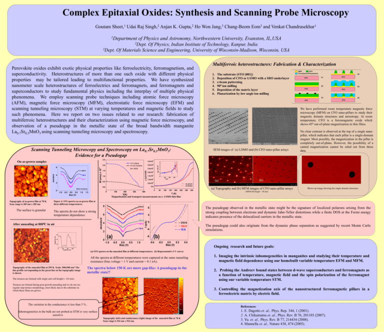
Complex Epitaxial Oxides: Synthesis and Scanning Probe Microscopy Goutam Sheet,1 Udai Raj Singh,2 Anjan K. Gupta,2 Ho Won Jang,3 Chang-Beom Eom3 and Venkat Chandrasekhar1 1Department of Physics and Astronomy, Northwestern University, Evanston, IL,USA 2Dept. Of Physics, Indian Institute of Technology, Kanpur, India 3Dept. Of Materials Science and Engineering, University of Wisconsin-Madison, Wisconsin, USA Perovskite oxides exhibit exotic physical properties like ferroelectricity, ferromagnetism, and superconductivity. Heterostructures of more than one such oxide with different physical properties may be tailored leading to multifunctional properties. We have synthesized nanometer scale heterostructures of ferroelectrics and ferromagnets, and ferromagnets and superconductors to study fundamental physics including the interplay of multiple physical phenomena. We employ scanning probe techniques including atomic force microscopy (AFM), magnetic force microscopy (MFM), electrostatic force microscopy (EFM) and scanning tunneling microscopy (STM) at varying temperatures and magnetic fields to study such phenomena. Here we report on two issues related to our research: fabrication of multiferroic heterostructures and their characterization using magnetic force microscopy, and observation of a pseudogap in the metallic state of the broad bandwidth manganite La0.7Sr0.3MnO3 using scanning tunneling microscopy and spectroscopy. Scanning Tunneling Microscopy and Spectroscopy on La0.7Sr0.3MnO3: On as-grown samples Evidence for a Pseudogap 295 K dlnI/dlnV 4 158 K 4 94 K 3.0x10 3 H = 10 G 2.5x10 3 2.0x10 3 1.5x10 3 1.0x10 3 5.0x10 2 1.5 1.0 0.5 Before Annealing -1.0 -0.5 0.0 0.5 Bias (V) 1.0 0 1.5 100 200 300 The spectra do not show a strong temperature dependence There is not much temperature The surface is granular due evolution. to a fast growth rate. After annealing at 8000C in air 310 K 255 K dlnI/dlnV 78 K Height (in nm) (a) -1.0 1.2 Terraces are formed during post-growth annealing and we do not see regular step-terrace morphology, most likely due to the substrate on which these films are grown. We have performed room temperature magnetic force microscopy (MFM) on CFO nano-pillars to study their magnetic domain structures and anisotropy. At room temperature, CFO is a ferromagnetic oxide which shows 450 out-of-plane magnetization in thin films. No clear contrast is observed at the top of a single nanopillar, which indicates that each pillar is a single-domain magnet. Most possibly, the magnetization in the pillar is completely out-of-plane. However, the possibility of a canted magnetization cannot be ruled out from these data. 0 -1 -2 100 200 300 T (K) (b) (a) as grown annealed 50 100 150 200 250 300 350 (a) Topography and (b) MFM images of CFO nano-pillar arrays Blown up image showing the single domain structures (MFM lift height = 30 nm) The pseudogap observed in the metallic state might be the signature of localized polarons arising from the strong coupling between electrons and dynamic Jahn-Teller distortions while a finite DOS at the Fermi energy indicates presence of the delocalized carriers in the metallic state. -4 -0.5 0.0 0.5 Bias (V) 78 K -0.4 1.0 The pseudogap could also originate from the dynamic phase separation as suggested by recent Monte Carlo simulations. (b) -0.2 0.0 0.2 Bias (V) 0.4 Ongoing research and future goals: 8 All the spectra at different temperatures were captured at the same tunneling resistance (bias voltage = 1 V 205 andKcurrent 4 = 0.1 nA). The spectra below 150 K are gap-like: A pseudogap in the 152 more K 0 310 K 4 metallic state!! 100 K 78 K 2 (a) 0 -1.0 I (pA) dlnI/dlnV Height (in nm) The terraces are formed with single unit cell height (~ 0.4 nm). STO (a) STS spectra on the annealed film at310 different temperatures. (b) Representative I-V curves K 6 40 80 120 Length (in nm) STO (6) 1 8 -8 255 K 0 (3) 2 152 K We may not see the inhomogeneities in the STM-S data310 asK 0 100 K the STM technique is very surface sensitive 152 K 4 0 On the samples annealed at 8000C in air Topography of the annealed film at 295 K.1.4Scale: 500x500 nm2 The line profile corresponding to the green line on the topography image 1.2 is shown. STO 3 205conductance K The variation in the is less than 5 % . 4 6 1.4 1.6 STO (5) Figure 5: Topography (left) and conductance (right) image of the annealed film at 78 K. 8 1.6 8 (2) T (K) 2 40 80 120 Length (in nm) STO Magnetization and transport measurements on a LSMO thin film -1.0 -0.5 0.0 0.5 1.0 1.5 Figure 4: STS spectra on as-grown film at Bias (V) three different temperatures. Figure 4: STS spectra on as-grown film at three different temperatures. 0 (1) 4 T(K) Before Annealing STO (4) 5 0 400 The substrate (STO [001]) Deposition of CFO or LSMO with a SRO underlayer e-beam patterning 900 ion milling Deposition of the matrix layer Planarization by low angle ion milling SRO CFO Ferroelectric/Piezoelectric 6 0.0 0.0 2 0 Figure 3: Topography of as-grwon The surface is granular film at 78 K. 94 K 2 0 Topography of as-grown film at 78 K. Scan range is 205 nm x 205 nm 158 K H in plane H out of plane 1. 2. 3. 4. 5. 6. SEM images of (a) LSMO and (b) CFO nano-pillar arrays I (pA) dlnI/dlnV 295 K 3 (-cm) 6 M (emu) x 10 6 -4 2.0 3.5x10 -7 On as-grown samples (d / dT) 10 2.5 Multiferroic heterostructures: Fabrication & Characterization -4 -8 -0.5 0.0 0.5 Bias (V) 1.0 152 K 78 K (b) -0.4 -0.2 0.0 0.2 Bias (V) The variation in the conductance is less than 5 % . 0.4 1. Imaging the intrinsic inhomogeneities in manganites and studying their temperature and magnetic field dependence using our homebuilt variable temperature EFM and MFM. 2. Probing the Andreev bound states between d-wave superconductors and ferromagnets as a function of temperature, magnetic field and the spin polarization of the ferromagnet using our variable temperature STM. 3. Controlling the magnetization axis of the nanostructured ferromagnetic pillars in a ferroelectric matrix by electric field. References: Inhomogeneities in the bulk are not probed as STM is very surface sensitive Topography (left) and conductance (right) image of the annealed film at 78 K. Scan range is 524 nm x 524 nm. 1. E. Dagotto et. al., Phys. Rep. 344, 1 (2001). 2. A. Chikamatsu et. al., Phys. Rev. B 76, 201103 (2007). 3. Yu. et. al., Phys. Rev. B 77, 214434 (2008). 4. Mannella et. al., Nature 438, 474 (2005).
