The Common-Source Amplifier Basic Circuit DC Solution
advertisement

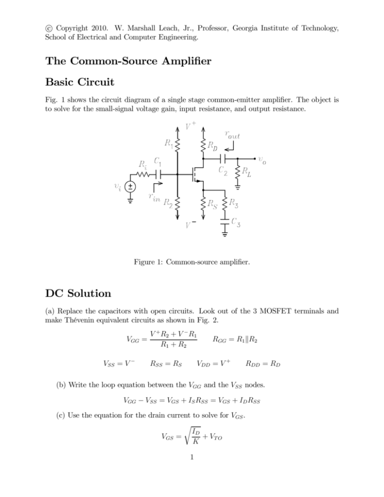
c Copyright 2010. W. Marshall Leach, Jr., Professor, Georgia Institute of Technology, ° School of Electrical and Computer Engineering. The Common-Source Amplifier Basic Circuit Fig. 1 shows the circuit diagram of a single stage common-emitter amplifier. The object is to solve for the small-signal voltage gain, input resistance, and output resistance. Figure 1: Common-source amplifier. DC Solution (a) Replace the capacitors with open circuits. Look out of the 3 MOSFET terminals and make Thévenin equivalent circuits as shown in Fig. 2. VGG = VSS = V − V + R2 + V − R1 R1 + R2 RGG = R1 kR2 VDD = V + RSS = RS RDD = RD (b) Write the loop equation between the VGG and the VSS nodes. VGG − VSS = VGS + IS RSS = VGS + ID RSS (c) Use the equation for the drain current to solve for VGS . r ID VGS = + VT O K 1 Figure 2: Bias circuit. (d) Solve the equations simultaneously. r ID ID RSS + + [(VGG − VSS ) − VT O ] = 0 K (e) Let V1 = (VGG − VSS ) − VT O . Solve the quadratic for ID . ¶2 µ√ 1 + 4KV1 RSS − 1 √ ID = 2 KRSS p (d) Verify that VDS > VGS − VT O = ID /K for the active mode. ¡ ¢ VDS = VD − VS = (VDD − ID RDD ) − V − + ID RSS = VDD − VSS − ID RDD Small-Signal or AC Solutions (a) Redraw the circuit with V + = V − = 0 and all capacitors replaced with short circuits as shown in Fig. 3. (b) Calculate gm , rs , and r0 from the DC solution. p gm = 2 KID rs = 1 gm r0 = λ−1 + VDS ID (c) Replace the circuits looking out of the gate and source with Thévenin equivalent circuits as shown in Fig. 4. vtg = vi R1 kR2 Ri + R1 kR2 Rtg = R1 kR2 2 vte = 0 Rts = RS kR3 Figure 3: Signal circuit. Figure 4: Signal circuit with Thévenin gate circuit. 3 Exact Solution (a) Replace the circuit seen looking into the drain with its Norton equivalent circuit as shown in Fig. 5. Solve for id(sc) . id(sc) = Gmg vtg = Gmg vi Gmg = R1 kR2 Ri + R1 kR2 r0 1 rs + Rts kr0 r0 + Rts Figure 5: Norton drain circuit. (b) Solve for vo . R1 kR2 rid kRD kRL Ri + R1 kR2 µ ¶ Rts r0 + rs kRts rid = = r0 1 + 0 + Rts 1 − Rts / (rs + Rte ) rs vo = −id(sc) rid kRD kRL = −Gmg vi (c) Solve for the voltage gain. Av = R1 kR2 vo = −Gms rid kRD kRL vi Ri + R1 kR2 (d) Solve for rin . rin = R1 kR2 (e) Solve for rout . rout = rid kRD (d) Special case for Rts = 0. Gmg = 1 = gm rs rid = r0 Example 1 For the CS amplifier of Fig. ??, it is given that Ri = 5 kΩ, R1 = 5 MΩ, R2 = 1 MΩ, RD = 10 kΩ, RS = 3 kΩ, R3 = 50 Ω, RL = 20 kΩ, V + = 24 V, V − = −24 V, K0 = 0.001 A/ V2 , VT O = 1.75 V, λ = 0.016 V−1 . Solve for the gain Av = vo /vi , the input resistance rin , and the output resistance rout . The capacitors can be assumed to be ac short circuits at the operating frequency. 4 Solution. For the dc bias solution, replace all capacitors with open circuits. The Thévenin voltage and resistance seen looking out of the gate are VGG = V + R2 + V − R1 = −16 V R1 + R2 RBB = R1 kR2 = 833.3 kΩ The Thévenin voltage and resistance seen looking out of the source are VSS = V − and RSS = RS . To calculate ID , we neglect the Early effect by setting K = K0 . The bias equation for ID is ¶2 µ√ 1 + 4KV1 RSS − 1 √ ID = = 1.655 mA 2 KRSS To test for the active mode, we calculate the drain-source voltage ¡ ¢ ¡ ¢ VDS = VD − VS = V + − ID RD − V − + ID RSS = 26.491 V p This must be greater than VGS − VT O = ID /K = 1.286 V. It follows that the MOSFET is biased in its active mode. For the small-signal ac analysis, we need gm , rs , and r0 . When the Early effect is accounted for, the new value of K is given by K = K0 (1 + λVDS ) = 1.424 × 10⁻³ A/ V2 Note that this is an approximation because the Early effect was neglected in calculating VDS . However, the approximation should be close to the true value. It follows that gm , rs , and r0 are given by p gm = 2 KID = 3.07 × 10⁻³ A/ V rs = 1 = 325.758 Ω gm λ−1 + VDS = 53.78 kΩ r0 = ID For the small-signal analysis, V + and V − are zeroed and the three capacitors are replaced with ac short circuits. The Thévenin voltage and resistance seen looking out of the gate are given by R1 kR2 vtg = vi = 0.994vi Rtg = Ri kR1 kR2 = 4.97 kΩ Ri + R1 kR2 The Thévenin resistances seen looking out of the source and the drain are Rts = RS kR3 = 49.18 Ω Rtd = RD kRL = 6.667 kΩ Next, we calculate Gmg and rid r0 1 1 S = rs + Rts kr0 r0 + Rts 375.237 µ ¶ Rts rid = r0 1 + + Rts = 61.95 kΩ rs Gmg = 5 The output voltage is given by vo = −Gmg × (rid kRtd ) vtg = −Gmg × (rid kRtd ) × 0.916vi = −15.945vi Thus the voltage gain is vo = −15.945 vi The input and output resistances are given by Av = rin = R1 kR2 = 833.3 kΩ rout = rid kRD = 8.61 kΩ Approximate Solutions These solutions assume that r0 = ∞ except in calculating rid . In this case, id(sc) = i0d = i0s . Source Equivalent Circuit Solution (a) After making the Thévenin equivalent circuits looking out of the gate and source, replace the MOSFET with the source equivalent circuit as shown in Fig. 6. Figure 6: Source equivalent circuit. (b) Solve for i0d = i0s and rid . vtg = i0s (re0 + Rte ) = i0d (rs + Rts ) =⇒ i0d = vtg 1 rs + Rts µ ¶ Rts r0 + rs kRts or rid = = r0 1 + 0 + Rts 1 − Rts / (rs + Rte ) rs (c) Solve for vo and Av = vo /vi . vo = −i0d rid kRD kRL = vtg −1 R1 kR2 1 rid kRD kRL = −vi rid kRD kRL rs + Rts Ri + R1 kR2 rs + Rts Rts = RS kR3 6 Av = Note that this is of the form 1 vo R1 kR2 =− rid kRD kRL vi Ri + R1 kR2 rs + Rts Av = vtg i0 i0 vo × s × d0 × 0 vi vtg is id (d) Solve for rout . rout = rid kRD Example 2 Use the simplified T-model solutions to calculate the values of Av , rin , and rout for Example 1. ¡ ¢ ¡ ¢ Av = 0.994 × 2.667 × 10−3 × −6.019 × 103 = −15.957 rin = 833.3 kΩ rid = 61.95 kΩ rout = 8.61 kΩ π Model Solution (a) After making the Thévenin equivalent circuits looking out of the gate and source, replace the MOSFET with the π model as shown in Fig. 7. Figure 7: Hybrid π model circuit. (b) Solve for i0d and rid . i0d vtg + i0d Rts =⇒ i0d = 1 gm + Rts gm µ ¶ Rts r0 + rs kRts = r0 1 + 0 + Rts rid = 1 − Rts / (rs + Rte ) rs vtg = vπ + i0s Rts = (c) Solve for vo . vo = −i0d rid kRD kRL = − vtg 1 + Rts gm rid kRD kRL = vi 7 R1 kR2 −rid kRD kRL Ri + R1 kR2 1 + Rts gm (d) Solve for the voltage gain. Av = 1 vo R1 kR2 = (−rid kRD kRL ) vi Ri + R1 kR2 1 + Rts gm This is of the form Av = vtg i0 vo × d × 0 vi vtg id (e) Solve for rin . rin = R1 kR2 (f) Solve for rout . rout = rid kRD Example 3 Use the π-model solutions to calculate the values of Av , rin , and rout for Example 1. ¡ ¢ ¡ ¢ Av = 0.994 × 2.667 × 10−3 × −6.019 × 103 = −15.957 rin = 833.3 kΩ rid = 61.95 kΩ rout = 8.61 kΩ T Model Solution (a) After making the Thévenin equivalent circuits looking out of the gate and source, replace the MOSFET with the T model as shown in Fig. 8. Figure 8: T model circuit. (b) Solve for i0d . vtg = i0s (rs + Rts ) = i0d (rs + Rts ) =⇒ i0d = vtg rs + Rts (c) Solve for vo . vo = −i0d rid kRD kRL = − R1 kR2 −rid kRD kRL vtg rid kRD kRL = vi rs + Rts Ri + R1 kR2 rs + Rts 8 (d) Solve for the voltage gain. Av = 1 vo R1 kR2 = (−rid kRD kRL ) vi Ri + R1 kR2 rs + Rts (e) Solve for rin . rin = R1 kR2 (f) Solve for rout . rout = rid kRD Example 4 Use the T-model solutions to calculate the values of Av , rin , and rout for Example 1. ¡ ¢ ¡ ¢ Av = 0.994 × 2.667 × 10−3 × −6.019 × 103 = −15.957 rin = 833.3 kΩ rid = 61.95 kΩ 9 rout = 8.61 kΩ


