!
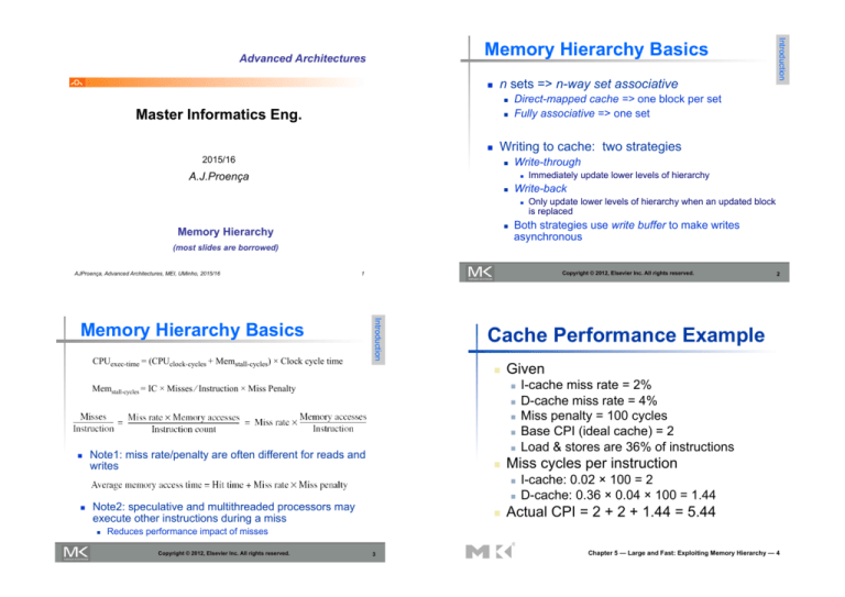
n sets => n-way set associative
!
Master Informatics Eng.
!
!
Introduction
Memory Hierarchy Basics
Advanced Architectures
Direct-mapped cache => one block per set
Fully associative => one set
Writing to cache: two strategies
2015/16
!
Write-through
!
Write-back
A.J.Proença
!
!
!
Memory Hierarchy
Immediately update lower levels of hierarchy
Only update lower levels of hierarchy when an updated block
is replaced
Both strategies use write buffer to make writes
asynchronous
(most slides are borrowed)
AJProença, Advanced Architectures, MEI, UMinho, 2015/16
Copyright © 2012, Elsevier Inc. All rights reserved.
1
CPUexec-time = (CPUclock-cycles + Memstall-cycles) × Clock cycle time
Introduction
Memory Hierarchy Basics
Cache Performance Example
!
Given
!
Memstall-cycles = IC × Misses ⁄ Instruction × Miss Penalty
!
!
!
!
!
Note1: miss rate/penalty are often different for reads and
writes
!
!
Note2: speculative and multithreaded processors may
execute other instructions during a miss
!
!
I-cache miss rate = 2%
D-cache miss rate = 4%
Miss penalty = 100 cycles
Base CPI (ideal cache) = 2
Load & stores are 36% of instructions
Miss cycles per instruction
!
!
2
I-cache: 0.02 × 100 = 2
D-cache: 0.36 × 0.04 × 100 = 1.44
Actual CPI = 2 + 2 + 1.44 = 5.44
Reduces performance impact of misses
Copyright © 2012, Elsevier Inc. All rights reserved.
3
Chapter 5 — Large and Fast: Exploiting Memory Hierarchy — 4
Miss rate
!
!
Fraction of cache access that result in a miss
Causes of misses (3C’s +1)
!
Compulsory
!
Capacity
!
!
!
!
Conflict
First reference to a block
Blocks discarded and later retrieved
Conflict
!
Program makes repeated references to multiple addresses
from different blocks that map to the same location in the
cache
Coherency
!
Different processors should see same value in same location
Copyright © 2012, Elsevier Inc. All rights reserved.
Cache Coherence
!
Coherence
!
!
All reads by any processor must return the most
recently written value
Writes to the same location by any two processors are
seen in the same order by all processors
(Coherence defines the behaviour of reads & writes to the
same memory location)
!
Consistency
!
!
When a written value will be returned by a read
If a processor writes location A followed by location B,
any processor that sees the new value of B must also
see the new value of A
6
Centralized Shared-Memory Architectures
Processors may see different values
through their caches:
Copyright © 2012, Elsevier Inc. All rights reserved.
5
Centralized Shared-Memory Architectures
The cache coherence pb
!
The 3C’s in diff cache sizes
Introduction
!
Introduction
Memory Hierarchy Basics
(Consistency defines the behaviour of reads & writes with
respect to accesses to other memory locations)
Copyright © 2012, Elsevier Inc. All rights reserved.
7
Copyright © 2012, Elsevier Inc. All rights reserved.
8
Coherent caches provide:
!
!
!
Migration: movement of data
Replication: multiple copies of data
Cache coherence protocols
!
Directory based
!
!
Sharing status of each block kept in one location
Memory Hierarchy Basics
!
!
Larger block size
!
!
Larger total cache capacity to reduce miss rate
!
Higher associativity
!
!
!
Giving priority to read misses over writes
!
Avoiding address translation in cache indexing
!
!
Given
!
!
!
!
!
!
Miss penalty = 100ns/0.25ns = 400 cycles
Effective CPI = 1 + 0.02 × 400 = 9
Now add L-2 cache …
!
!
10
!
Penalty = 5ns/0.25ns = 20 cycles
Primary miss with L-2 miss
!
!
Access time = 5ns
Global miss rate to main memory = 0.5%
Primary miss with L-2 hit
!
!
Chapter 5 — Large and Fast: Exploiting Memory Hierarchy — 11
Reduces hit time
Now add L-2 cache
!
With just primary cache
!
Reduces miss penalty
Example (cont.)
!
CPU base CPI = 1, clock rate = 4GHz
Miss rate/instruction = 2%
Main memory access time = 100ns
Reduces overall memory access time
Copyright © 2012, Elsevier Inc. All rights reserved.
9
Multilevel Cache Example
Reduces conflict misses
Increases hit time, increases power consumption
Multilevel caches to reduce miss penalty
!
Copyright © 2012, Elsevier Inc. All rights reserved.
Increases hit time, increases power consumption
!
!
Each core tracks sharing status of each block
Reduces compulsory misses
Increases capacity and conflict misses, increases miss penalty
!
!
Snooping
!
Six basic cache optimizations:
Introduction
!
Centralized Shared-Memory Architectures
Enforcing Coherence
Extra penalty = 400 cycles
CPI = 1 + 0.02 × 20 + 0.005 × 400 = 3.4
Performance ratio = 9/3.4 = 2.6
Chapter 5 — Large and Fast: Exploiting Memory Hierarchy — 12
Multilevel On-Chip Caches
3-Level Cache Organization
Intel Nehalem 4-core processor
Intel Nehalem
AMD Opteron X4
L1 caches
(per core)
L1 I-cache: 32KB, 64-byte
blocks, 4-way, approx LRU
replacement, hit time n/a
L1 D-cache: 32KB, 64-byte
blocks, 8-way, approx LRU
replacement, write-back/
allocate, hit time n/a
L1 I-cache: 32KB, 64-byte
blocks, 2-way, approx LRU
replacement, hit time 3 cycles
L1 D-cache: 32KB, 64-byte
blocks, 2-way, approx LRU
replacement, write-back/
allocate, hit time 9 cycles
L2 unified
cache
(per core)
256KB, 64-byte blocks, 8-way,
512KB, 64-byte blocks, 16-way,
approx LRU replacement, write- approx LRU replacement, writeback/allocate, hit time n/a
back/allocate, hit time n/a
L3 unified
cache
(shared)
8MB, 64-byte blocks, 16-way,
replacement n/a, write-back/
allocate, hit time n/a
2MB, 64-byte blocks, 32-way,
replace block shared by fewest
cores, write-back/allocate, hit
time 32 cycles
n/a: data not available
Per core: 32KB L1 I-cache, 32KB L1 D-cache, 512KB L2 cache
Chapter 5 — Large and Fast: Exploiting Memory Hierarchy — 14
!
!
!
Small and simple first level caches
!
small & simple first-level caches
way-prediction
!
!
!
!
pipelined cache access
nonblocking caches
multibanked caches
!
Reducing the miss penalty
!
!
!
critical word first
merging write buffers
!
Reducing the miss rate
!
Reducing the miss penalty or miss rate via parallelism
!
!
!
Critical timing path:
!
Increase cache bandwidth
!
!
!
Reducing the hit time
!
1. Small and simple 1st level caches
addressing tag memory, then
comparing tags, then
selecting correct set
Advanced Optimizations
Ten Advanced Optimizations
Direct-mapped caches can overlap tag compare and
transmission of data
Lower associativity reduces power because fewer
cache lines are accessed
compiler optimizations
hardware prefetching of instructions and data
compiler-controlled prefetching
AJProença, Advanced Architectures, MEI, UMinho, 2015/16
15
Copyright © 2012, Elsevier Inc. All rights reserved.
16
L1 Size and Associativity
Access time vs. size and associativity
Copyright © 2012, Elsevier Inc. All rights reserved.
To improve hit time, predict the way to pre-set
mux
!
!
Mis-prediction gives longer hit time
Prediction accuracy
!
!
!
!
!
!
Copyright © 2012, Elsevier Inc. All rights reserved.
17
> 90% for two-way
> 80% for four-way
I-cache has better accuracy than D-cache
3. Pipelining Cache
!
Pipeline cache access to improve bandwidth
!
Examples:
!
!
!
!
First used on MIPS R10000 in mid-90s
Used on ARM Cortex-A8
!
Pentium: 1 cycle
Pentium Pro – Pentium III: 2 cycles
Pentium 4 – Core i7: 4 cycles
18
Advanced Optimizations
!
Energy per read vs. size and associativity
Advanced Optimizations
2. Way Prediction
Advanced Optimizations
Advanced Optimizations
L1 Size and Associativity
Increases branch mis-prediction penalty
Makes it easier to increase associativity
Extend to predict block as well
!
!
Way selection
Increases mis-prediction penalty
Copyright © 2012, Elsevier Inc. All rights reserved.
19
Copyright © 2012, Elsevier Inc. All rights reserved.
20
Allow hits before
previous misses
complete
!
!
!
!
Hit under miss
Hit under multiple
miss
L2 must support this
In general,
processors can hide
L1 miss penalty but
not L2 miss penalty
Copyright © 2012, Elsevier Inc. All rights reserved.
Critical word first
!
!
!
Early restart
!
!
!
Request missed word from memory first
Send it to the processor as soon as it arrives
!
ARM Cortex-A8 supports 1-4 banks for L2
Intel i7 supports 4 banks for L1 and 8 banks for L2
Interleave banks according to block address
Copyright © 2012, Elsevier Inc. All rights reserved.
7. Merging Write Buffer
!
!
!
When storing to a block that is already pending in the
write buffer, update write buffer
Reduces stalls due to full write buffer
Do not apply to I/O addresses
22
No write
buffering
Effectiveness of these strategies depends on
block size and likelihood of another access to
the portion of the block that has not yet been
fetched
Copyright © 2012, Elsevier Inc. All rights reserved.
!
21
Request words in normal order
Send missed work to the processor as soon as it
arrives
Organize cache as independent banks to
support simultaneous access
Advanced Optimizations
!
!
!
Advanced Optimizations
6. Critical Word First, Early Restart
5. Multibanked Caches
Advanced Optimizations
!
Advanced Optimizations
4. Nonblocking Caches
Write buffering
23
Copyright © 2012, Elsevier Inc. All rights reserved.
24
Loop Interchange
!
!
Swap nested loops to access memory in
sequential order
9. Hardware Prefetching
!
Fetch two blocks on miss (include next
sequential block)
Advanced Optimizations
!
Advanced Optimizations
8. Compiler Optimizations
Blocking
!
!
Instead of accessing entire rows or columns,
subdivide matrices into blocks
Requires more memory accesses but improves
locality of accesses
Pentium 4 Pre-fetching
Copyright © 2012, Elsevier Inc. All rights reserved.
!
!
Insert prefetch instructions before data is
needed
Non-faulting: prefetch doesn t cause
exceptions
Loads data into register
Cache prefetch
!
!
Summary
26
Register prefetch
!
!
Copyright © 2012, Elsevier Inc. All rights reserved.
Advanced Optimizations
!
Advanced Optimizations
10. Compiler Prefetching
25
Loads data into cache
Combine with loop unrolling and software
pipelining
Copyright © 2012, Elsevier Inc. All rights reserved.
27
Copyright © 2012, Elsevier Inc. All rights reserved.
28
