Review: Cache Optimization 5 Basic cache optimizations
advertisement
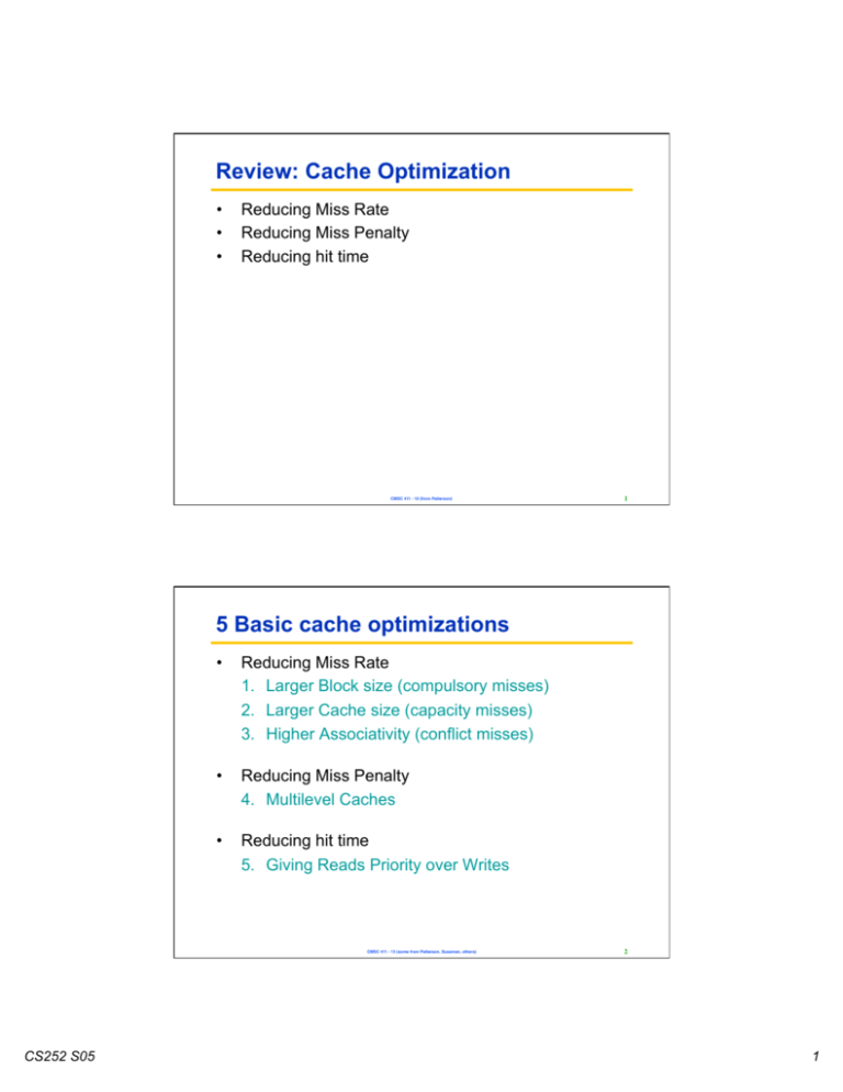
Review: Cache Optimization • • • Reducing Miss Rate Reducing Miss Penalty Reducing hit time CMSC 411 - 10 (from Patterson) 1 5 Basic cache optimizations • Reducing Miss Rate 1. Larger Block size (compulsory misses) 2. Larger Cache size (capacity misses) 3. Higher Associativity (conflict misses) • Reducing Miss Penalty 4. Multilevel Caches • Reducing hit time 5. Giving Reads Priority over Writes CMSC 411 - 13 (some from Patterson, Sussman, others) CS252 S05 2 1 Review: cont. • Victim caches • Trace caches • Hardware prefetch CMSC 411 - 10 (from Patterson) 3 Memory Hierarchy 3 (Main Memory & Virtual Memory) CS252 S05 2 Main memory management • Questions: – How big should main memory be? – How to handle reads and writes? – How to find something in main memory? – How to decide what to put in main memory? – If main memory is full, how to decide what to replace? CMSC 411 - 14 (some from Patterson, Sussman, others) 5 The scale of things • Typically (as of 2012): – Registers: < 1 KB, access time .25–.5 ns – L1 Cache: < 8 MB, access time 1–5 ns – Main Memory: ~4 GB, access time 10–50 ns – Disk Storage: ~2TB, access time 10 ms • Memory Technology – CMOS (Complementary Metal Oxide Semiconductor) – Uses a combination of n- and p-doped semiconductor material to achieve low power dissipation. CMSC 411 - 14 (some from Patterson, Sussman, others) CS252 S05 6 3 Memory hardware • DRAM: dynamic random access memory, typically used for main memory – One transistor per data bit – Each bit must be refreshed periodically (e.g., every 8 milliseconds), so maybe 5% of time is spent in refresh – Access time < cycle time – Address sent in two halves so that fewer pins are needed on chip (row and column access) CMSC 411 - 14 (some from Patterson, Sussman, others) 7 Memory hardware (cont.) • SRAM: static random access, typically used for cache memory – 4-6 transistors per data bit – No need for refresh – Access time = cycle time – Address sent all at once, for speed CMSC 411 - 14 (some from Patterson, Sussman, others) CS252 S05 8 4 Bottleneck • Main memory access will slow down the CPU unless the hardware designer is careful • Some techniques can improve memory bandwidth, the amount of data that can be delivered from memory in a given amount of time: – Wider main memory – Interleaved memory – Independent memory banks – Avoiding memory bank conflicts CMSC 411 - 14 (some from Patterson, Sussman, others) 9 Wider main memory • Wider cache lines – Cache miss: If a cache block contains k words, then each cache miss involves these steps repeated k times: » Send the address to main memory » Access the word (i.e., locate it) » Send the word to cache, with the bits transmitted in parallel – Idea behind wider memory: the user thinks about 32 bit words, but physical memory can have longer words – Then the operations above are done only k/n times, where n is the number of 32 bit words in a physical word CMSC 411 - 14 (some from Patterson, Sussman, others) CS252 S05 10 5 Wider main memory (cont.) • Extra costs: – A wider memory bus: hardware to deliver 32n bits in parallel, instead of 32 bits – A multiplexer to choose the correct 32 bits to transmit from the cache to the CPU 11 CMSC 411 - 14 (some from Patterson, Sussman, others) Interleaved memory • Partition memory into banks, with each bank able to access a word and send it to cache in parallel • Organize address space so that adjacent words live in different banks - called interleaving • For example, 4 banks might have words with the following octal addresses: Bank 0 Bank 1 Bank 2 Bank3 00 01 02 03 04 05 06 07 10 11 12 13 … … … … CMSC 411 - 14 (some from Patterson, Sussman, others) CS252 S05 12 6 Interleaved memory (cont.) • Note how nice interleaving is for write-through • Also helps speed read and write-back • Note: Interleaved memory acts like wide memory, except that words are transmitted through the bus sequentially, not in parallel CMSC 411 - 14 (some from Patterson, Sussman, others) 13 Independent memory banks • Each bank of memory has its own address lines and (usually) a bus • Can have several independent banks: perhaps – One for instructions – One for data – This is called a Harvard architecture • Banks can operate independently without slowing others CMSC 411 - 14 (some from Patterson, Sussman, others) CS252 S05 14 7 Avoid memory bank conflicts • By having a prime number of memory banks • Since arrays frequently have even dimension sizes and often dimension sizes that are a power of 2 strides that match the number of banks (or a multiple) give very slow access CMSC 411 - 14 (some from Patterson, Sussman, others) 15 Example: Interleaving int x[256][512]; for (j=0; j<512; j=j+1) for (i=0; i<256; i=i+1) x[i][j] = 2 * x[i][j]; • First access the first column of x: – x[0][0], x[1][0], x[2][0], ... x[255][0] • with addresses – K, K+512*4, K+512*8, ... K +512*4*255 • With 4 memory banks, all of the elements live in the same memory bank, so the CPU will stall in the worst possible way CMSC 411 - 14 (some from Patterson, Sussman, others) CS252 S05 16 8 How much good do these techniques do? • Example: Assume a cache block of 4 words, and – 4 cycles to send address to main memory – 24 cycles to access a word, once the address arrives – 4 cycles to send a word back to cache • Basic miss penalty: 4*32 = 128 cycles, since each of 4 words has the full 32 cycle penalty • Memory with a 2-word width: 2*(32+4) = 72 cycle miss penalty • Simple interleaved memory: address can be sent to each bank simultaneously, so miss penalty is 4 + 24 + 4*4 (for sending words) = 44 cycles • Independent memory banks: 32 cycle miss penalty, as long as the words are in different banks, since each has its own address lines and bus CMSC 411 - 14 (some from Patterson, Sussman, others) 17 Virtual addressing • Computers are designed so that multiple programs can be active at the same time • At the time a program is compiled, the compiler has to assign addresses to each data item. But how can it know what memory addresses are being used by other programs? • Instead, the compiler assigns virtual addresses, and expects the loader/OS to provide the means to map these into physical addresses CMSC 411 - 15 (some from Patterson, Sussman, others) CS252 S05 18 9 Memory protection • Each program “lives” in its own virtual space, called its process • When the CPU is working on one process, others may be partially completed or waiting for attention • The CPU is time shared among the processes, working on each in turn • And main memory is also shared among processes CMSC 411 - 15 (some from Patterson, Sussman, others) 19 In the olden days … • The loader would locate an unused set of main memory addresses and load the program and data there • There would be a special register called the relocation register, and all addresses that the program used would be interpreted as addresses relative to the base address in that register • So if the program jumped to location 54, the jump would really be to 54 + contents of relocation register. A similar thing, perhaps with a second register, would happen for data references CMSC 411 - 15 (some from Patterson, Sussman, others) CS252 S05 20 10 In the less-olden days ... • It became difficult to find a contiguous segment of memory big enough to hold program and data, so the program was divided into pages, with each page stored contiguously, but different pages in any available spot, either in main memory or on disk • This is the virtual addressing scheme – to the program, memory looks like a contiguous segment, but actually, data is scattered in main memory and perhaps on disk CMSC 411 - 15 (some from Patterson, Sussman, others) 21 But we know all about this! • Already know that a program and data can be scattered between cache memory and main memory • Now add the reality that its location in main memory is also determined in a scattered way, and some pages may also be located on disk • So each page has its own relocation value CMSC 411 - 15 (some from Patterson, Sussman, others) CS252 S05 22 11 Virtual addressing Virtual memory CMSC 411 - 15 (some from Patterson, Sussman, others) CS252 S05 24 12 Parameters Parameter First-level cache Virtual memory Block (page) size 16-128 bytes 4096-65,536 bytes Hit time 1-3 clock cycles 50-150 cc Miss penalty 8-200 cc 106-107 cc (access time) (6-160 cc) (.8-8)*106 cc (transfer time) (2-40 cc) (.2-2)*106 cc Miss rate 0.1-10% 0.00001-0.001% Address mapping 25-45 bit physical address to 14-20 bit cache address 32-64 bit virtual address to 25-45 bit physical address CMSC 411 - 15 (some from Patterson, Sussman, others) 25 Cache vs. virtual memory Cache Cache miss handled by hardware Cache size fixed for a particular machine Fundamental unit is a block Cache fault Virtual memory Page faults handled by operating system Virtual memory size fixed for a particular program Fundamental unit is a fixed-length page or a variable-length segment Page fault CMSC 411 - 15 (some from Patterson, Sussman, others) CS252 S05 26 13 Old protection mode: base & bound • User processes need to be protected from each other • Two registers, base and bound test whether this virtual address belongs to this process • If not, a memory protection violation exception is raised • Users cannot change the base and bound registers bound P1 bound base P2 base CMSC 411 - 15 (some from Patterson, Sussman, others) 27 Who can change them? • The operating system needs access to the base and bound registers • So a process that is labeled kernel (also called supervisor or executive) can access any memory location and change the registers • Kernel processes are accessed through system calls, and a return to user mode is like a subroutine return, restoring the state of the user process CMSC 411 - 15 (some from Patterson, Sussman, others) CS252 S05 28 14 Segmentation • Basically multiple base&bounds – w/ virtual memory stack bound Process stack base Each segment can be located anywhere in physical memory heap bound heap base CMSC 411 - 15 (some from Patterson, Sussman, others) CS252 S05 29 15
