®
ByteBlasterMV Parallel Port
Download Cable
June 1999, ver. 1.01
Features
Data Sheet
■
■
■
■
■
■
The ByteBlasterMV™ parallel port download cable (ordering code:
PL-BYTEBLASTERMV) is a hardware interface to a standard PC parallel
port (also known as an LPT port). This cable drives configuration data to
APEX 20K, FLEX 10K (including FLEX 10KA and FLEX 10KE),
FLEX 8000, and FLEX 6000 devices, as well as programming data to
MAX 9000, MAX 7000S, MAX 7000A, and MAX 3000A devices. Because
design changes are downloaded directly to the device, prototyping is easy
and multiple design iterations can be accomplished in quick succession.
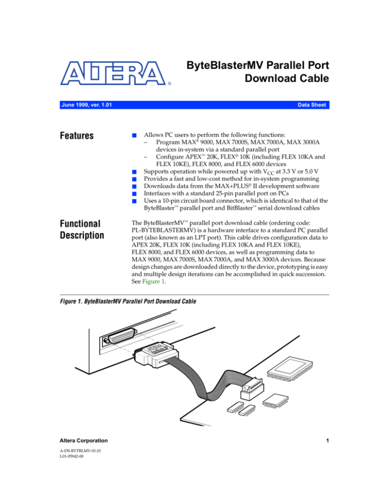
See Figure 1.
Figure 1. ByteBlasterMV Parallel Port Download Cable
ByteB
Altera Corporation
A-DS-BYTBLMV-01.01
L01-05942-00
laster
MV
1
13
Development
Tools
Functional
Description
Allows PC users to perform the following functions:
– Program MAX® 9000, MAX 7000S, MAX 7000A, MAX 3000A
devices in-system via a standard parallel port
– Configure APEX™ 20K, FLEX® 10K (including FLEX 10KA and
FLEX 10KE), FLEX 8000, and FLEX 6000 devices
Supports operation while powered up with VCC at 3.3 V or 5.0 V
Provides a fast and low-cost method for in-system programming
Downloads data from the MAX+PLUS® II development software
Interfaces with a standard 25-pin parallel port on PCs
Uses a 10-pin circuit board connector, which is identical to that of the
ByteBlaster™ parallel port and BitBlaster™ serial download cables
ByteBlasterMV Parallel Port Download Cable Data Sheet
Download Modes
The ByteBlasterMV cable provides two download modes:
■
■
Passive serial (PS) mode—Used for configuring APEX 20K,
FLEX 10K, FLEX 8000, and FLEX 6000 devices
JTAG mode—Industry-standard Joint Test Action Group (JTAG)
interface for programming or configuring APEX 20K, FLEX 10K,
MAX 9000, MAX 7000S, MAX 7000A, and MAX 3000A devices
ByteBlasterMV Connections
The ByteBlasterMV cable has a 25-pin male header that connects to the PC
parallel port, and a 10-pin female plug that connects to the circuit board.
Data is downloaded from the PC’s parallel port through the
ByteBlasterMV cable to the circuit board via the connections discussed in
this section.
1
To configure 2.5-V APEX 20K and FLEX 10KE devices using the
ByteBlasterMV download cable, connect the pull-up resistors to
a 3.3-V power supply, the cable’s VCC pin to a 3.3-V power
supply, and the device’s VCCINT pin to a 2.5-V power supply. For
PS configuration, the device’s VCCIO pin must be connected to a
2.5-V or 3.3-V power supply. The ByteBlasterMV VCC pin must
be connected to 3.3 V for either APEX 20K and FLEX 10KE JTAG
configuration, or MAX 7000A and MAX 3000A JTAG in-system
programming. The device VCCIO pin can be connected to either
a 2.5-V or 3.3-V power supply.
ByteBlasterMV Header & Plug Connections
The 25-pin male header connects to a parallel port with a standard parallel
cable. Table 1 identifies the pins and the download modes.
Table 1. ByteBlasterMV 25-Pin Header Pin-Outs
Pin
2
PS Mode Signal Name
JTAG Mode Signal Name
2
DCLK
TCK
3
nCONFIG
TMS
8
DATA0
TDI
11
CONF_DONE
TDO
13
nSTATUS
–
15
VCC
VCC
18 to 25
GND
GND
Altera Corporation
ByteBlasterMV Parallel Port Download Cable Data Sheet
Figure 2 shows a schematic of the ByteBlasterMV download cable.
Figure 2. ByteBlasterMV Schematic
10-Pin Plug Connections
VCC
(2)
VCC
4
VCC
7
(2)
25-Pin Male Header
Connections
3
74HC244
14
(1)
9
(1)
GND
(1)
VCC VCC VCC
(2)
2
3
(1)
(1)
8
(1)
(2)
(1)
(2)
GND
GND
VCC
GND
1A1
1Y1
1A2
1Y2
1A3
1Y3
1A4
1Y4
2A1
2A2
2Y1
2Y2
2A3
2Y3
2A4
2Y4
GND
(1)
(1)
1
5
(1)
9
13
Development
Tools
7
VCC
1G
2G
2, 10
10
GND
13
(1)
11
(1)
12
(1)
VCC
15
(2)
18-25
GND
Notes:
(1)
(2)
All series resistors are 100 Ω.
All pull-up resistors are 2.2 KΩ.
The 10-pin female plug connects to a 10-pin male header on the circuit
board containing the target device(s). Figure 3 shows the dimensions of
the female plug.
Altera Corporation
3
ByteBlasterMV Parallel Port Download Cable Data Sheet
Figure 3. ByteBlasterMV 10-Pin Female Plug Dimensions
Dimensions are shown in inches. The spacing between pin centers is 0.1 inch.
0.425 Typ.
Color Strip
1
3
5
7
9
2
4
6
8
10
0.250 Typ.
0.100 Sq.
0.025 Sq.
0.700 Typ.
Table 2 identifies the 10-pin female plug’s pin names for the
corresponding download mode.
Table 2. ByteBlasterMV Female Plug’s Pin Names & Download Modes
Pin
PS Mode
Signal Name
Signal Name
Description
1
DCLK
Clock signal
TCK
Clock signal
2
GND
Signal ground
GND
Signal ground
3
CONF_DONE
Configuration
control
TDO
Data from device
4
VCC
Power supply
VCC
Power supply
5
nCONFIG
Configuration
control
TMS
JTAG state
machine control
6
–
No connect
–
No connect
7
nSTATUS
Configuration
status
–
No connect
8
–
No connect
–
No connect
9
DATA0
Data to device
TDI
Data to device
GND
Signal ground
GND
Signal ground
10
1
4
Description
JTAG Mode
The circuit board must supply VCC and ground to the
ByteBlasterMV cable.
Altera Corporation
ByteBlasterMV Parallel Port Download Cable Data Sheet
Circuit Board Header Connection
The ByteBlasterMV 10-pin female plug connects to a 10-pin male header
on the circuit board. The 10-pin male header has two rows of five pins,
which are connected to the device’s programming or configuration pins.
The ByteBlasterMV cable receives power and downloads data via the
male header. Figure 4 shows the dimensions of a typical 10-pin male
header.
Figure 4. 10-Pin Male Header Dimensions
Dimensions are shown in inches.
Top View
Side View
0.100
0.100
0.025 Sq.
0.235
13
The Tables 3 through 5 summarize the absolute maximum ratings,
recommended operating conditions, and DC operating conditions for the
ByteBlasterMV cable.
Table 3. ByteBlasterMV Cable Absolute Maximum Ratings
Min
Max
Unit
VCC
Symbol
Supply voltage
Parameter
With respect to ground
Conditions
–0.5
7.0
V
VI
DC input voltage
With respect to ground
–0.5
7.0
V
Table 4. ByteBlasterMV Cable Recommended Operating Conditions
Symbol
VCC
Min
Max
Unit
Supply voltage, 5.0-V operation
Parameter
4.5
5.5
V
Supply voltage, 3.3-V operation
3.0
3.6
V
Altera Corporation
Conditions
5
Development
Tools
Operating
Conditions
ByteBlasterMV Parallel Port Download Cable Data Sheet
Table 5. ByteBlasterMV Cable DC Operating Conditions
Symbol
Parameter
Conditions
Min
Max
Unit
VIH
High-level input voltage
VCC = 4.5 V
3.15
VCC = 3.0 V
2.1
VIL
Low-level input voltage
VCC = 4.5 V
VOH
5.0-V high-level TTL output voltage
TTL load. VCC = 4.5 V, IOH = 8 mA
3.80
V
3.3-V high-level TTL output voltage
TTL load. VCC = 3.0 V, IOH = 4 mA
2.48
V
5.0-V high-level CMOS output
voltage
CMOS load. VCC = 4.5 V, IOH = 50 µA
4.4
V
3.3-V high-level CMOS output
voltage
CMOS load. VCC = 3.0 V, IOH = 50 µA
2.9
V
5.0-V low-level TTL output voltage
TTL load. VCC = 4.5 V, IOL = 8 mA
0.44
3.3-V low-level TTL output voltage
TTL load. VCC = 3.0 V, IOL = 4 mA
0.44
V
5.0-V low-level CMOS output voltage CMOS load. VCC = 4.5 V, IOL = 50 µA
0.1
V
3.3-V low-level CMOS output voltage CMOS load. VCC = 3.0 V, IOL = 50 µA
0.1
V
Operating current
50
mA
1.35
VCC = 3.0 V
VOL
ICC
Software
Instructions
V
V
0.9
V
The MAX+PLUS II Programmer downloads configuration or
programming data for FLEX 10K, FLEX 8000, FLEX 6000, MAX 9000,
MAX 7000S, MAX 7000A, or MAX 3000A devices.
1
For Quartus™ Programmer instructions, please refer to Quartus
Help.
To configure or program one or more devices with the ByteBlasterMV
cable and the MAX+PLUS II Programmer, follow these steps:
1.
Compile a project. The MAX+PLUS II Compiler automatically
generates an SOF for FLEX 10K, FLEX 8000, and FLEX 6000 device
configuration, or a POF for MAX 9000, MAX 7000S, MAX 7000A, and
MAX 3000A device programming.
2.
Attach the ByteBlasterMV cable to a parallel port on a PC and insert
the 10-pin female plug into the prototype system containing the
target device. The board must supply power to the ByteBlasterMV
cable.
1
6
For the Windows NT operating system, a driver must be installed
before using the ByteBlasterMV cable. Go to the MAX+PLUS II
Getting Started Manual for instructions on installing
ByteBlasterMV drivers.
Altera Corporation
ByteBlasterMV Parallel Port Download Cable Data Sheet
3.
Open the MAX+PLUS II Programmer. Choose the Hardware Setup
command (Options menu) to specify the ByteBlasterMV cable and
the appropriate LPT port. See “Changing the Hardware Setup” in
MAX+PLUS II Help for more information.
1
4.
The MAX+PLUS II software automatically loads the
programming file for the current project (either a POF or SOF),
or the first programming file for a multi-device project. To
specify another programming file, choose Select Programming
File (File menu) and specify the correct file. For a FLEX 10K,
FLEX 8000, or FLEX 6000 device, select an SOF; for a MAX 9000,
MAX 7000S, MAX 7000A, or MAX 3000A device, select a POF.
For JTAG or FLEX-chain programming or configuration, perform the
following steps:
v To program or configure devices in a JTAG chain (multi- or
single-device chain), turn on Multi-Device JTAG-Chain (JTAG
menu) and choose Multi-Device JTAG Chain Setup to set up
the multi-device JTAG chain. See “Setting up Multi-Device
JTAG Chains” in MAX+PLUS II Help for more information.
If the JTAG chain includes either FLEX or MAX devices
exclusively, set up and create just one JTAG Chain File (.jcf).
Likewise, if the JTAG chain includes a mixture of FLEX and
MAX devices, set up and create two separate JCFs. One JCF
will configure the FLEX devices, and the other JCF will
program the MAX devices.
v To configure multiple devices in a FLEX chain, turn on MultiDevice FLEX Chain (FLEX menu) and choose Multi-Device
FLEX Chain Setup to set up the multi-device FLEX chain. See
“Setting Up Multi-Device FLEX Chains” in MAX+PLUS II Help
for more information.
5.
Choose the Program or Configure button to program or configure
the device(s).
The ByteBlasterMV cable downloads the data from the SOF or POF File(s)
into the device(s).
Conclusion
Altera Corporation
Downloading configuration and programming data directly to the device
via the ByteBlasterMV cable allows designers to verify multiple design
iterations in quick succession, thereby speeding the design cycle.
7
Development
Tools
1
13
ByteBlasterMV Parallel Port Download Cable Data Sheet
References
For more information on configuration and in-system programmability
(ISP), see the following sources:
■
■
■
■
■
■
Revision
History
The information contained in the ByteBlasterMV Parallel Port Download
Cable Data Sheet version 1.01 supersedes information published in
previous versions. The ByteBlasterMV Parallel Port Download Cable Data
Sheet version 1.01 contains the following changes:
■
■
■
■
■
■
■
■
8
Application Note 116 (Configuring APEX 20K, FLEX 10K & FLEX 6000
Devices)
Application Note 33 (Configuring FLEX 8000 Devices)
Application Note 38 (Configuring Multiple FLEX 8000 Devices)
Application Note 39 (IEEE 1149.1 (JTAG) Boundary-Scan Testing in
Altera Devices)
Application Note 95 (In-System Programmability in MAX Devices)
Search for “Configuring a Single Device with the BitBlaster,
ByteBlaster, or FLEX Download Cable,” “Setting Up Multi-Device
JTAG Chains,” ”Configuring Multiple Devices in a JTAG Chain with
the BitBlaster or ByteBlaster,” and “Programming Multiple Devices
in a JTAG Chain with the BitBlaster or ByteBlaster” in MAX+PLUS II
Help.
Information on APEX 20K and MAX 3000A devices were added
throughout the document.
JTAG configuration information for APEX 20K and FLEX 10KE
devices was updated in the “ByteBlasterMV Connections” section on
page 2.
JTAG ISP configuration information for MAX 7000A and MAX 3000A
devices was added to the “ByteBlasterMV Connections” section on
page 2.
The “Passive Serial Mode” section was removed. This information is
found in Application Note 116 (Configuring APEX 20K, FLEX 10K &
FLEX 6000 Devices).
The “JTAG Mode” section was removed. This information is found in
Application Note 39 (IEEE 1149.1 (JTAG) Boundary-Scan Testing in
Altera Devices) and Application Note 95 (In-System Programmability in
MAX Devices).
The Quartus software was added to the “Software Instructions”
section.
The “References” section was added, and provides sources for
additional information on the ByteBlasterMV download cable.
Minor textual, illustration, and style changes were made to the data
sheet.
Altera Corporation
Copyright © 1995, 1996, 1997, 1998, 1999 Altera Corporation, 101 Innovation Drive,
San Jose, CA 95134, USA, all rights reserved.
By accessing this information, you agree to be bound by the terms of Altera’s
Legal Notice.


