Real-Time Challenges
and Opportunities in SoCs
WP-01190-1.1
White Paper
Advanced process technology and system-integration provide the driving forces
behind silicon convergence. FPGAs speed along this trajectory, having already
integrated SRAM memories, digital signal processing (DSP) and multiplier blocks,
serial transceivers, memory controllers, and advanced I/O functions. The latest
advancement in programmable technology is the SoC, which integrates an Altera®
FPGA with an ARM® applications processor, plus a rich peripheral processor
subsystem. The convergence of these technologies provides new challenges and
opportunities for real-time embedded system design.
Introduction
This white paper explores an advanced motor drive or inverter application to
illustrate how silicon convergence affects real-time design. Before the advent of
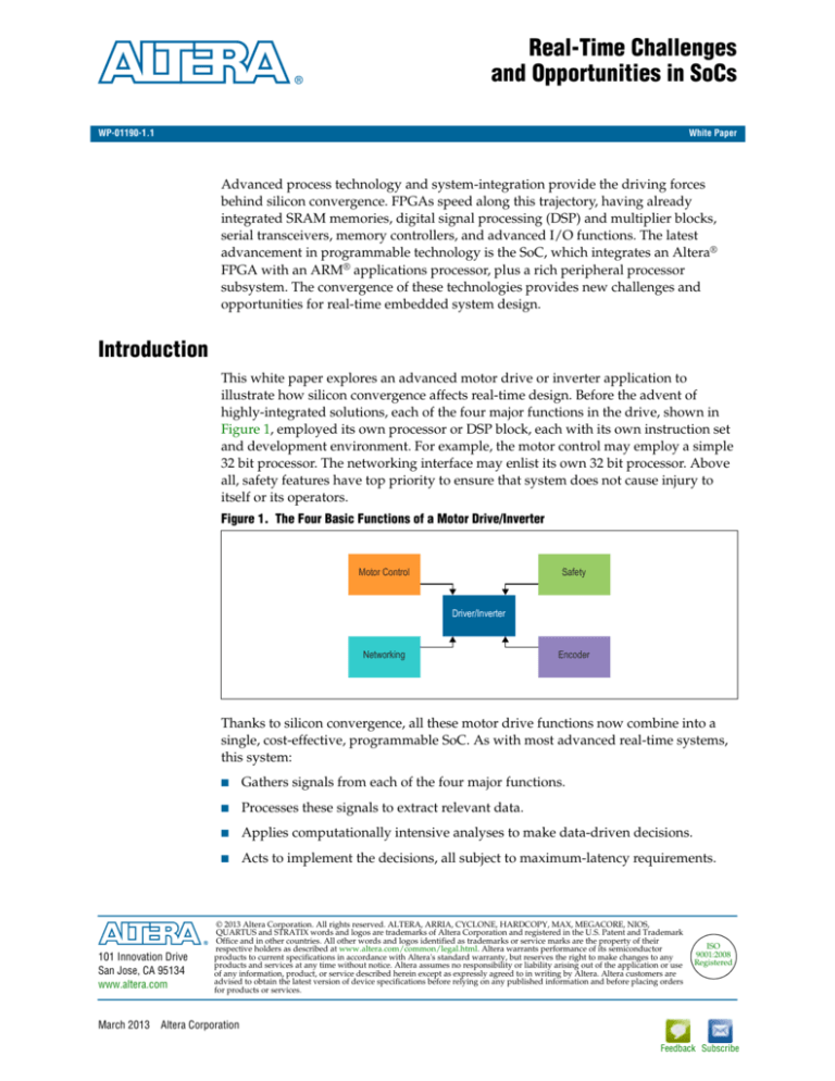
highly-integrated solutions, each of the four major functions in the drive, shown in
Figure 1, employed its own processor or DSP block, each with its own instruction set
and development environment. For example, the motor control may employ a simple
32 bit processor. The networking interface may enlist its own 32 bit processor. Above
all, safety features have top priority to ensure that system does not cause injury to
itself or its operators.
Figure 1. The Four Basic Functions of a Motor Drive/Inverter
Motor Control
Safety
Driver/Inverter
Networking
Encoder
Thanks to silicon convergence, all these motor drive functions now combine into a
single, cost-effective, programmable SoC. As with most advanced real-time systems,
this system:
101 Innovation Drive
San Jose, CA 95134
www.altera.com
March 2013
■
Gathers signals from each of the four major functions.
■
Processes these signals to extract relevant data.
■
Applies computationally intensive analyses to make data-driven decisions.
■
Acts to implement the decisions, all subject to maximum-latency requirements.
© 2013 Altera Corporation. All rights reserved. ALTERA, ARRIA, CYCLONE, HARDCOPY, MAX, MEGACORE, NIOS,
QUARTUS and STRATIX words and logos are trademarks of Altera Corporation and registered in the U.S. Patent and Trademark
Office and in other countries. All other words and logos identified as trademarks or service marks are the property of their
respective holders as described at www.altera.com/common/legal.html. Altera warrants performance of its semiconductor
products to current specifications in accordance with Altera's standard warranty, but reserves the right to make changes to any
products and services at any time without notice. Altera assumes no responsibility or liability arising out of the application or use
of any information, product, or service described herein except as expressly agreed to in writing by Altera. Altera customers are
advised to obtain the latest version of device specifications before relying on any published information and before placing orders
for products or services.
ISO
9001:2008
Registered
Altera Corporation
Feedback Subscribe
Page 2
Challenge—Doing Ever More in Less Time
This same real-time processing model appears in other diverse applications such as
automotive driver assistance, real-time financial trading, and guidance systems.
Challenge—Doing Ever More in Less Time
System responsiveness is a driving force in real-time applications. How quickly and
consistently can a system respond to real-time events? Can the system perform its
necessary tasks within a specific, bounded time, every time? Embedded engineers
continually seek to perform ever more sophisticated functions and calculations but in
less total time.
Initially, the embedded hardware performed simple proportional-integral-derivative
(PID) motor control. Over time, motor control became more sophisticated to include
model-based motor control solutions, as shown in Figure 2. Motion-adaptive motor
control allows the system to intelligently adapt to changing systems conditions and
retune control parameters based on sensor feedback. Lastly, in a factory automation
environment, multiple motors communicate to coordinate their response and
complex movements. For example, a safety-related exception may trigger a shutdown sequence that requires coordinated movements of a variety of equipment to
protect both the operator and downstream machinery to minimize system downtime.
Naturally, all of this sophisticated computing happens in ever-decreasing amounts of
time.
Figure 2. Embedded Applications Asked to Do Ever More in Less Time
Processing
DSP Performance
Simple PID
Motor
Control
ModelBased
Motor
Control
MotionAdaptive
Motor
Control
Functional
Safety
(Hard
Real-Time)
As the algorithms grow in sophistication, they also require more computations, larger
data sets, and more DSP power. The location of stored data and the communication
bandwidth to that data has major implications and directly affects system
responsiveness.
March 2013
Altera Corporation
Real-Time Challenges and Opportunities in SoCs
Challenge—Scheduling Conflicts
Page 3
Challenge—Scheduling Conflicts
Scheduling conflicts are another inevitable challenge in real-time system design. In
traditional design approaches, each of the four major motor drive functions shown in
Figure 3 has its own dedicated processor and each essentially operates independently.
In a converged solution, these four functional groups are combined into a single
system but each still operates asynchronously. Potential scheduling conflicts occur
because all of the interrupts are routed to a single device. If not handled properly, the
random and asynchronous nature of the interrupts potentially causes scheduling
clashes within the application program, resulting in decreased responsiveness.
Managing jitter and ensuring more-deterministic behavior are key factors to avoid
schedule conflicts.
Figure 3. Motor Drive Application
Safety
Networking
Position/
Velocity Control
10 μs
~2 μs
Current/
Voltage Control
If the entire motor drive application is integrated within a single processor, the
majority of its computing time is spent performing the current control loop, shown in
purple in Figure 3. Meanwhile, as the system performs its various other motor control
and networking functions, a safety event may be triggered within the system. The
system must detect the fault condition, diagnose it, respond immediately to take the
appropriate safety action, and shut down gracefully because safety has the highest
overall priority. How fast the system can actually respond is key.
Measuring System Responsiveness
How is real-time responsiveness measured? Responsiveness consists of two elements:
■
Interrupt latency—Once an event happens, how quickly can the system recognize
it? For processor- or DSP-based applications, the interrupt latency (I) is the period
from the moment an interrupt is asserted to the instant that the processor
completes its currently executing machine instruction and branches to the first line
of the interrupt service routine (ISR).
■
Execution time—After the event is recognized, how quickly can the system process
it? For processor- or DSP-based applications, execution time (E) is the amount of
time required for the processor to complete all the instructions within a particular
ISR and then return to normal operation.
Real-Time Challenges and Opportunities in SoCs
March 2013
Altera Corporation
Page 4
Real-Time Processors and Tools
The total response time adds the interrupt latency to the interrupt execution time
(I + E), as illustrated in Figure 4.
Figure 4. Interrupt Latency and Process Execution Time
Interrupt
Occurs
Interrupt Is Recognized
and Execution Begins
Interrupt Process
Returns
Time
I
(Interrupt Latency)
E
(Interrupt Process Execution Time)
Real-Time Processors and Tools
Altera’s programmable technologies provide unique capabilities to speed algorithms
and opportunities that improve a system’s real-time response. Time-critical
algorithms can be efficiently partitioned between highly parallel hardware solutions
implemented on programmable logic elements (LEs), DSP blocks, or software
solutions executed on one or more hard or soft processors
Altera’s real-time processors and tools, summarized in Table 1, enable embedded
system designers to explore hardware/software tradeoffs and to develop new
solutions that meet demanding real-time performance challenges. The solution to
meet real-time challenges lies within the careful partitioning of real-time algorithms
between hardware and software implementations across Altera’s real-time processors
and tools, which comprise:
■
Hard processors (ARM Cortex™-A9 processors)
■
Soft real-time processors (Nios® II processors)
■
DSP blocks (variable-precision hardware multipliers and accumulators)
■
State machines (custom hardware using LEs within core fabric)
Table 1. Altera Real-Time Tools Components
Solution
ARM Cortex-A9
Processor
Nios II Soft Processor
DSP Builder +
Intellectual Property (IP)
Hardware-Based State
Machines
March 2013
Altera Corporation
Interrupt Latency
Execution Speed
Data Sets
Derterminism
Design
Method
Moderate
High
Very large
Moderate
C
Low
(vectored interrupt
controller)
Moderate
Large
High
C
Low
High to
very high
Limited
Very high
(no jitter)
MATLAB/
Simulink
Very low
Extremely high
Small
Very high
(no jitter)
FPGA design,
HDL tools
Real-Time Challenges and Opportunities in SoCs
Real-Time Processors and Tools
Page 5
Altera’s ARM Cortex-A9-based hard processor subsystem (HPS) potentially improves
real-time performance in systems where execution speed or throughput dominates
the real-time response time. Exploiting asymmetric multiprocessing (AMP)
techniques, one Cortex-A9 processor typically executes the operating system and
main application program while the second Cortex-A9 processor is dedicated to the
time-critical, real-time function.
Altera’s Nios II soft processor utilizes the resources of the FPGA. The maximum clock
frequency for Nios II processors is constrained by the core fabric performance of a
given FPGA. For example, in Cyclone® V devices, 100 – 150 MHz Nios II processor
clock rates are common. The Nios II processor offers some distinct advantages for
real-time processing, including:
■
Low interrupt latency thanks to a vectored interrupt controller.
■
The number of possible Nios II processors in an application is limited only by the
size of the FPGA fabric.
■
A single highly time-critical function can be dedicated to a single Nios II processor,
guaranteeing highly deterministic interrupt response times and freeing the ARM
Cortex-A9 processor for other functions.
■
Nios II processor has the ability to use on-chip memory as tightly coupled
memory, which is useful to store critical real-time algorithms.
■
Nios II processors have custom instruction interfaces that allow FPGA hardwarebased accelerators to implement a real-time function and return the result directly
to the processor pipeline.
Altera’s variable-precision DSP architecture provides the most powerful real-time
performance in systems where matrix manipulations, filters, transforms, and DSP
operations dominate the real-time response time. The highly parallel nature of the
FPGA’s programmable architecture plus an abundance of variable-precision DSP
blocks coupled with block SRAMs delivers extreme performance for many
applications. For example, Altera’s Stratix® series FPGAs offer over 1 teraFLOPS
(TFLOPS) of floating-point DSP performance, which greatly exceeds the performance
of any ARM-based processor and only rivaled by high-end GPUs.
1
See the “Achieving 1 TFLOPS Performance with 28 nm FPGAs” webcast for
additional information.
Altera’s DSP Builder design software, a plug-in to the popular MATLAB/Simulink
software, empowers designers to use model-based entry methods to generate RTL
automatically and to evaluate tradeoffs between fixed-point and floating-point
performance and dynamic range. Similarly, designers can unroll loops for maximum
performance or fold them, allowing logic reuse that conserves FPGA resources.
Finally, for ultimate performance and determinism, the FPGA core fabric and
adaptive logic modules (ALMs) provide fast, efficient hardware-based state machines.
Via custom-crafted designs in VHDL or Verilog HDL, the FPGA can deliver
unparalleled response times for specific applications and for applications with
smaller data sets. However, the design engineer requires knowledge of HDL and the
design constraints for timing closure.
Real-Time Challenges and Opportunities in SoCs
March 2013
Altera Corporation
Page 6
Benchmark Example—FOC
Benchmark Example—FOC
The performance gains achieved from hardware/software tradeoffs are entirely
application dependent and nothing highlights these effects better than a real-world
benchmark example. This motor-control benchmark example uses field-oriented
control (FOC), shown in Figure 5, where the algorithm consists of two types of control
loops. The outer control loops measure the position and velocity of the motor and
requires low processing rates, making it ideal for traditional processor-based
solutions.
Figure 5. FOC Benchmark
SVM
Inner Control Loop
Position
Request
Position
PI Control
Speed PI
Control
Torque
PI Control
Vq
Inverse
Park
Flux PI Vd Transform
Control
Pulse
Width
Modulation
Park
Transform
Clarke
Transform Ib
Current
Feedback
ADC
Interface
Position
Speed
Outer Control Loop
Motor
Inverter
Ia
Iq
Id
Va
Inverse Vb
Clarke
Transform Vc
Encoder
Interface
ADC
Position Feedback
Position
Sensor
(Encoder)
Interface IP
In contrast, the inner control loop is far more computationally complex and
demanding. Relying on current feedback measurements from the motor, the inner
control loop calculates torque and flux using Park and Clarke data transforms and
their inverse operations. The resulting torque and flux calculations ultimately
produce a space-vector modulation (SVM) value that drives the motor. The inner loop
operations require much higher processing rates and are computationally complex.
This benchmark example is implemented using the following hardware versus
software solutions available in an SoC:
■
Implement the FOC benchmark solely using the ARM Cortex-A9 processor using
C code.
■
Implement the FOC benchmark solely using a Nios II soft processor using C code.
■
Apply hardware acceleration techniques that leverage FPGA-based Nios II
processing and DSP Builder.
■
Explore fixed-point vs. floating-point solutions.
■
Explore solutions with unrolled and folded critical loops.
Finally, the resulting solutions are compared and contrasted for their real-time
response and deterministic behavior.
March 2013
Altera Corporation
Real-Time Challenges and Opportunities in SoCs
Solution 1—ARM Cortex-A9 Processor Only
Page 7
Solution 1—ARM Cortex-A9 Processor Only
In this implementation, the entire FOC motor control benchmark code is written in C
and implemented exclusively on the SoC’s ARM Cortex-A9 MPCore™ processor. The
design is a “bare metal” solution without an operating system, which avoids the
potential additional ambiguities introduced by an operating system.
Cortex-A9 Interrupt Response Characteristics
The main factors that affect the Cortex-A9 processor’s response time are interrupts.
As shown in Figure 4, the Cortex-A9 processor within an SoC accepts interrupts from
ARM’s Generic Interrupt Controller (GIC). Interrupts are steered to one or both of the
CPUs. The GIC is designed primarily for ARM’s application-class processors. ARM’s
real-time processors, the Cortex-R and Cortex-M families, employ a vectored
interrupt controller that provides lower interrupt latency.
Figure 6. Dual-Core Cortex-A9 MPCore Processor on a SoC
Generic Interrupt Controller
IEEE 745 Floating-Point
Support (VFPU)
IEEE 745 Floating-Point
Support (VFPU)
NEON DSP/Media
Processing Engine
NEON DSP/Media
Processing Engine
800 MHz
ARM Cortex-A9
32 bit Dual-Issue
Superscalar RISC CPU
800 MHz
ARM Cortex-A9
32 bit Dual-Issue
Superscalar RISC CPU
32 KB
Data
L1 Cache
32 KB
Data
L1 Cache
32 KB
Instruction
L1 Cache
32 KB
Instruction
L1 Cache
512 KB L2 Unified Cache with ECC
DDR Memory Controller (with ECC Support)
An interrupt event can happen at any time. However, the ARM CPU will not
recognize the interrupt event until the currently executing machine instruction
completes, as shown in Figure 7. At 800 MHz, each instruction generally finishes
quickly but the biggest variance is the access time to the data the CPU is currently
processing. For example, accesses to processor registers are the fastest, followed by
access to the L1 cache. Similarly, access to the L2 cache access is slower, and slowest is
the access to external memory that happens just as the DDR memory controller begins
a refresh cycle. Once the interrupt is recognized, the Cortex-A9 processor speeds
through the ISR at 800 MHz.
Real-Time Challenges and Opportunities in SoCs
March 2013
Altera Corporation
Page 8
Solution 1—ARM Cortex-A9 Processor Only
Imagine if a safety-critical interrupt event arrives just as the background application
code decides to blink a non-critical status LED, whose state variable is stored in
external DDR memory that just happens to be in the middle of its refresh cycle. The
high-priority interrupt must wait until the CPU finishes the current instruction—
blinking a non-critical LED! How can a designer avoid such situations?
Figure 7. Interrupt Latency Depends on Data Access of Current Instruction
Interrupt Event Not Recognized Until
Current Instruction Completes. Maximum
Interrupt Latency Depends on Current
Instruction and Data Access Type.
Recognize Interrupt Event
and Branch to ISR
Processor
Register
L1 Data
Cache
L2 Unified Cache
ISR
DDR Memory Controller
Refresh
Cycle
DDR Memory Controller
Complete Current Instruction
Execute ISR
The worst-case interrupt latency depends on the worst-case data access type.
Constraining the data access types will reduce the interrupt latency. There are two
CPUs in the SoC’s dual-core processor. Using AMP techniques, dedicate one
processor to fast interrupt response for time-critical, real-time functions while using
the remaining processor for the operating system, application program, and
communication.
The following three examples demonstrate how the interrupt response time is affected
by constraining the background code and the ISR to fast memory. Of course, for
ultimate performance, the background code should be a while(1) loop.
All of these examples use the FOC benchmark as their critical code. All
implementations are “bare-metal” solutions to eliminate the additional uncertainty
imposed by an operating system. While the selected FOC benchmark code was run as
bare-metal code in AMP mode for this case study, a popular use of the dual-core ARM
Cortex-A9 processor is as a single execution engine (in symmetric multiprocessing
(SMP) mode) with an RTOS or a high-level OS, such as Linux, for process handling.
March 2013
Altera Corporation
Real-Time Challenges and Opportunities in SoCs
Solution 1—ARM Cortex-A9 Processor Only
Page 9
The Best Case Scenario—Critical Code and Background Code Constrained
to <32 KB
The best possible interrupt response on the dual-core ARM Cortex-A9 processor
happens by dedicating one of the two CPUs to handling the critical interrupt, as
shown in Figure 8. The background code and critical code must be constrained to
32 KB or less so that it fits entirely within the CPU’s L1 instruction cache and all data
structures must be allocated to registers or to the CPU’s L1 data cache.
Figure 8. Best ARM Cortex-A9 Interrupt Response: Critical and Background Code <32 KB
High-Priority Interrupt
IEEE 745 Floating-Point
Support (VFPU)
IEEE 745 Floating-Point
Support (VFPU)
NEON DSP/Media
Processing Engine
NEON DSP/Media
Processing Engine
800 MHz
ARM Cortex-A9
32 bit Dual-Issue
Superscalar RISC CPU
800 MHz
ARM Cortex-A9
32 bit Dual-Issue
Superscalar RISC CPU
32 KB
Data
L1 Cache
32 KB
Data
L1 Cache
32 KB
Instruction
L1 Cache
32 KB
Instruction
L1 Cache
Table 2 shows the results of the FOC benchmark test when the code executes directly
from the L1 cache. The average is the result of 1,024 individual runs of the interrupt
routine. The jitter is the difference between the fastest and slowest responses. With
this partitioning, the interrupt response time is less than 1 µs, as shown in Table 2 and
Figure 9, which is amazingly good for an application processor without a vectored
interrupt controller. The primary reason for the exceptional performance is the
Cortex-A9 processor, as the SoC speeds through the ISR at 800 MHz.
Table 2. ARM Cortex-A9 Interrupt Response Time (Code <32 KB)
Minimum
Average
Maximum
Jitter
Interrupt Latency, I (µs)
0.16
0.170
0.19
0.03
FOC Benchmark Code, E (µs)
0.70
0.705
0.73
0.03
Total ISR Execution Time, I+E (µs)
0.86
0.875
0.92
0.06
Real-Time Challenges and Opportunities in SoCs
March 2013
Altera Corporation
Page 10
Solution 1—ARM Cortex-A9 Processor Only
Figure 9. ARM Cortex-A9 Interrupt Response Time (Code <32 KB)
2.5
2.0
1.5
1.0
0.5
0.0
0.92
0.86
0.875
0.70
0.71
0.73
0.16
0.17
0.19
Minimum
Average
Maximum
The ARM Cortex-AP interrupt response time is quite consistent, with little jitter or
variation between the minimum and maximum times—just 0.06 µs or 60 ns! Although
this special case technique provides excellent interrupt response times, it may not be
applicable for all applications. After all, there is only one additional ARM Cortex-A9
processor available in the SoC and the interrupt routines must all fit entirely within
32 KB. Unlike the FPGA-based solutions described later, this technique can be used
just once in a design without incurring slower performance. Adding other ISRs will
likely push the code beyond the 32 KB limit, slowing the overall response.
March 2013
Altera Corporation
Real-Time Challenges and Opportunities in SoCs
Solution 1—ARM Cortex-A9 Processor Only
Page 11
Critical Code and Background Code <256 KB
While the FOC benchmark code used in this article fits nicely within a 32 KB limit, not
all interrupt routines are so fortunate. The next performance boundary ensures that
the code and data fit within 256 KB of the L2 cache, as shown in Figure 10. The SoC
allows code and data to be locked in the cache, guaranteeing fast access for critical
routines.
Figure 10. Critical and Background Code <256 KB
High-Priority Interrupt
IEEE 745 Floating-Point
Support (VFPU)
IEEE 745 Floating-Point
Support (VFPU)
NEON DSP/Media
Processing Engine
NEON DSP/Media
Processing Engine
800 MHz
ARM Cortex-A9
32 bit Dual-Issue
Superscalar RISC CPU
800 MHz
ARM Cortex-A9
32 bit Dual-Issue
Superscalar RISC CPU
32 KB
Data
L1 Cache
32 KB
Data
L1 Cache
32 KB
Instruction
L1 Cache
32 KB
Instruction
L1 Cache
256 KB L2 Unified
Cache with ECC
In this evaluation, the L1 caches were flushed to emulate eviction that occurs when a
large background task (>32 KB) is running. After an interrupt event happens, the
background task may need to access data held in the L2 cache to complete its current
machine instruction before the CPU recognizes the interrupt. Consequently, there is
up to nearly an 8X increase in interrupt latency (I) as shown in Table 3 and Figure 11—
from a best case of 0.165 µs to a worst case of 1.30 µs.
Table 3. ARM Cortex-A9 Interrupt Response Time (Code <256 KB)
Minimum
Average
Maximum
Jitter
Interrupt Latency, I (µs)
0.165
0.86
1.30
1.135
FOC Benchmark Code, E (µs)
0.700
0.71
0.79
0.090
Total ISR Execution Time, I+E (µs)
0.865
1.57
2.09
1.225
Real-Time Challenges and Opportunities in SoCs
March 2013
Altera Corporation
Page 12
Solution 1—ARM Cortex-A9 Processor Only
Figure 11. Interrupt Response: Critical and Background Code <256 KB
2.5
2.09
2.0
0.79
1.57
1.5
0.71
1.0
0.865
1.30
0.5
0.0
0.700
0.86
0.165
Minimum
Average
Maximum
Comparing Table 2 and Table 3, the ISR requires slightly more time under these
conditions because of slower access to L2 cache for some operations. In the previous
example, where the entire code and data fit within 32 KB, the total response time was
less because the interrupt handler fit entirely in the L1 cache.
It is evident from Figure 11 that there is far more jitter or variation in the interrupt
response compared to the best-case scenario—up to 1.215 µs in jitter. However, the
total worst-case interrupt response remains a very respectable 2.09 µs.
March 2013
Altera Corporation
Real-Time Challenges and Opportunities in SoCs
Solution 1—ARM Cortex-A9 Processor Only
Page 13
Critical Code and Data <256 KB, Background Code >256 KB
This last example assumes that the background code and data are too large to fit
within the L2 cache and require access to external DDR memory, as shown in
Figure 12. The critical interrupt handler code remains less than 256 KB and is locked
in the L2 cache. The L1 and L2 caches accelerate data accesses to external DDR
memory. However, in the worst case, some accesses will be delayed while the DDR
memory controller is performing a refresh cycle. A DDR memory refresh operation
adds another 200 ns to the total access time.
Figure 12. Critical and Data <256 KB, Background Code >256 KB
High-Priority Interrupt
IEEE 745 Floating-Point
Support (VFPU)
IEEE 745 Floating-Point
Support (VFPU)
NEON DSP/Media
Processing Engine
NEON DSP/Media
Processing Engine
800 MHz
ARM Cortex-A9
32 bit Dual-Issue
Superscalar RISC CPU
800 MHz
ARM Cortex-A9
32 bit Dual-Issue
Superscalar RISC CPU
32 KB
Data
L1 Cache
32 KB
Data
L1 Cache
32 KB
Instruction
L1 Cache
32 KB
Instruction
L1 Cache
256 KB L2 Unified
Cache with ECC
DDR Memory Controller (up to 4 GB)
with ECC Support
Because the critical code is less than 256 KB and is held in the L2 cache, the FOC
benchmark code still executes quickly. The entire interrupt response, even with a
background task that accesses external memory, remains a respectable 2.29 µs, as
shown in Table 4.
Table 4. ARM Cortex-A9 Interrupt Response Time (Critical and Data <256 KB, Background Code >256 KB)
Minimum
Average
Maximum
Jitter
Interrupt Latency, I (µs)
0.41
0.89
1.50
1.09
FOC Benchmark Code, E (µs)
0.70
0.71
0.79
0.09
Total ISR Execution Time, I+E (µs)
1.11
1.60
2.29
1.18
Real-Time Challenges and Opportunities in SoCs
March 2013
Altera Corporation
Page 14
Solution 1—ARM Cortex-A9 Processor Only
As shown in Figure 13, the possible refresh delay increases the maximum interrupt
response time but actually slightly decreases the total jitter compared to the previous
scenario.
Figure 13. Interrupt Response: Critical and Data <256 KB, Background Code >256 KB
2.5
2.29
2.0
0.79
1.60
1.5
1.11
0.71
1.0
0.70
1.50
0.5
0.89
0.41
0.0
Minimum
Average
Maximum
Summary of ARM Cortex-A9 Results
Examining the results of the Cortex-A9 benchmark implementations, a few key points
stand out:
March 2013
■
Interrupt latency is directly affected by the location of data accesses by the
background task.
■
For best performance, dedicate one of the two Cortex-A9 processors to exclusively
handling critical interrupt routines.
■
Ensure that only critical loops are executed on the Cortex-A9 processor dedicated
to critical routines. Other background tasks affect the interrupt latency to handle
the critical routine.
■
Interrupt execution time (E) is dominated by the code location and processor clock
frequency.
■
For best determinism, keep the critical routine to <32K and keep it in the L1 cache.
■
For the best compromise between code size and performance, keep the critical
routine to <256 KB and lock it in the L2 cache.
Altera Corporation
Real-Time Challenges and Opportunities in SoCs
Solution 2—Stand-Alone Nios II Processor Running FOC Algorithm
Page 15
Solution 2—Stand-Alone Nios II Processor Running FOC Algorithm
Each SoC has a maximum of two ARM Cortex-A9 processors. Even when one is
dedicated to critical routines, the application might require multiple, simultaneous,
time-critical operations. A relatively simple method to offload the critical function
while maintaining full C code compatibility is to use a Nios II soft processor.
For the best real-time response, the critical code executes from a tightly-coupled block
RAM memory in the FPGA fabric, as shown in Figure 14. Similarly, the vectored
interrupt controller soft IP should be used for the lowest interrupt latency (I). Because
the Nios II processor is built from FPGA fabric, the maximum performance is
governed by the maximum performance of the underlying FPGA architecture—a
Cyclone V or Arria® V device. For this benchmark example, the Nios II processor ran
at a conservative 100 MHz, although 150 MHz performance is readily achievable in
Cyclone V FPGAs.
Figure 14. Nios II Soft Processor Configured for Best Real-Time Response (No DSP Builder
Acceleration)
Vector Interrupt
Controller IP
Nios II
Soft Processor
Critical Code
Stored in
Tightly-Coupled
Block RAM
In this implementation, the FOC benchmark used fixed-point arithmetic. Because the
Nios II soft processor is dedicated to exclusively handling the FOC benchmark, the
Nios II processor is not burdened by any background tasks. Consquently, the Nios II
solution provides nearly absolute determinism with little or no jitter (Table 5), even
across thousands of test runs.
Table 5. Nios II Soft Processor Interrupt Response Time, No Acceleration
Minimum
Average
Maximum
Jitter
Interrupt Latency, I (µs)
0.93
0.93
0.93
0
FOC Benchmark Code, E (µs)
4.50
4.50
4.50
0
Total ISR Execution Time, I+E (µs)
5.43
5.43
5.43
0
As shown in Figure 15, although the 100 MHz Nios II soft processor solution does not
deliver the blazing-fast execution time of the 800 MHz ARM Cortex-A9 processor, it
does furnish results that compare favorably to a popular 180 MHz ARM Cortex-R4F
processor, specifically designed for good real-time performance. Like the Nios II
solution, the Cortex-R4F has a vectored interrupt controller to reduce interrupt
latency. Regardless, the Nios II soft processor solution completes its interrupt
Real-Time Challenges and Opportunities in SoCs
March 2013
Altera Corporation
Page 16
Solution 2—Stand-Alone Nios II Processor Running FOC Algorithm
response in well under 10 µs—the measure of “goodness” for this high-performance
motor control application example. The Nios II FOC execution time can be further
reduced by using custom instructions to offload the processor. For example, a
trigonometric custom instruction can take 3 µs off of the 4.5 µs while still maintaining
zero jitter.
Figure 15. Interrupt Response: Nios II Solution Without Acceleration Compared to Cortex-A9 MPCore and Cortex-R4F
Processors
5.5
5.43
5.0
4.88
4.5
4.0
3.5
4.50
3.0
3.84
2.5
2.09
2.0
0.79
1.5
1.0
0.92
0.5
0.73
0.0
0.19
ARM Cortex-A9
at 800 MHz
< 32 KB (Max)
1.30
ARM Cortex-A9
at 800 MHz
< 256 KB (Max)
2.29
0.79
1.50
ARM Cortex-A9
at 800 MHz < 256 KB
Background
> 256 KB (Max)
1.04
0.93
Popular ARM
Cortex-R4F
at 180 MHz (Max)
Nios II at 100 MHz,
Vectored Interrupt
Controller, No
Acceleration
Thanks to its vectored interrupt controller, the Nios II interrupt latency is faster than
the other solutions except for the best-case scenario with a dedicated Cortex-A9
processor with less than 32 KB of critical code. Generally, the Nios II solution
responds quickly, especially when the most timing-critical operations are packed into
the earlier instructions within the ISR.
March 2013
Altera Corporation
Real-Time Challenges and Opportunities in SoCs
Solution 3—FOC Algorithm Partitioned Between Hardware and Software
Page 17
Solution 3—FOC Algorithm Partitioned Between Hardware and
Software
In Solution 2, the entire FOC benchmark was executed as software on a Nios II soft
processor, including the inner control loops. Can the FPGA logic inside an SoC
accelerate the overall application? In these next few examples, the outer control loops
of the FOC benchmark that monitor position and velocity execute in software on the
Nios II soft processor, as shown in Figure 16. However, the performance-critical inner
control loop functions execute using FPGA hardware accelerators created using DSP
Builder, part of the Altera real-time design tools. These accelerated functions include
the Park and Clarke transforms and their inverse operations plus the SVM function.
Figure 16. FOC Benchmark Using Hardware and Software Partitioning
SVM
Inner Control Loop
DSP Builder
Position
Request
Position
PI Control
Speed PI
Control
Torque
PI Control
Vq
Inverse
Park
Flux PI Vd Transform
Control
Pulse
Width
Modulation
Park
Transform
Clarke
Transform Ib
Current
Feedback
ADC
Interface
Position
Speed
Motor
Inverter
Ia
Iq
Id
Va
Inverse Vb
Clarke
Transform Vc
Encoder
Interface
ADC
Position Feedback
Position
Sensor
(Encoder)
Nios II Software
FPGA
Interface IP
Outer Control Loop
Real-Time Challenges and Opportunities in SoCs
March 2013
Altera Corporation
Page 18
Solution 3—FOC Algorithm Partitioned Between Hardware and Software
Figure 17 shows the general block diagram for each of the following solutions. The
Nios II soft processor handles the outer loops and controls data flow to and from the
FPGA-based hardware accelerators. The inner loops are offloaded to FPGA-based
hardware accelerators crafted with DSP Builder. The Nios II soft processor sends data
and commands to the hardware accelerators over an Avalon® Memory-Mapped
(Avalon-MM) interconnect bus.
Figure 17. Nios II Solution with DSP Builder Hardware Accelerators
Vector Interrupt
Controller IP
Nios II
Soft Processor
Avalon-MM
Interconnect
DSP Builder
Hardware
Accelerator
Critical Code
Stored in
Tightly-Coupled
Block RAM
The Avalon-MM interconnect incurs additional latency—the number of clock cycles
required for data to traverse the interconnect logic from the Nios II soft processor to
the accelerated function built with DSP Builder. The additional latency also increases
the total interrupt latency (I). It is also possible to pipeline the hardware accelerator
across multiple axes, as the total latency for 1, 2, 4, or even 16 axes of FOC control does
not scale linearly and new axis results per clock cycle are obtained after the initial
latency has been paid. In a processor-only implementation, the increase is linear as the
number of axes increases.
FPGA-based hardware accelerators encourage a variety of implementation styles. For
example, via DSP Builder, a design engineer can choose between solutions that offer
the best hardware efficiency, the lowest latency, or the maximum performance. DSP
Builder supports both fixed-point or floating-point solutions. Floating-point
calculations incur additional clock cycles but also provide much wider dynamic
range, while fixed-point calculations are faster and require fewer resources.
DSP Builder also empowers the designer to trade off the FPGA resources consumed
by a particular function against additional latency incurred by logic reuse taking
advantage of the relatively high FPGA clock frequency relative to the required
throughput. Critical loops can be unrolled or unfolded for maximum performance,
but at the cost of extra resources. Folding the critical loops conserves FPGA resources,
but at the cost of additional clock cycles. Folding provides up to a 10X resource
savings.
March 2013
Altera Corporation
Real-Time Challenges and Opportunities in SoCs
Solution 3—FOC Algorithm Partitioned Between Hardware and Software
Page 19
Table 6 and Figure 18 show the performance advantages of the various hardware
acceleration solutions. All the examples leverage the same Nios II soft processor core
with the vectored interrupt controller. The baseline comparison is the software-only
Nios II solution without any DSP Builder acceleration.
Table 6. Nios II Solution with Hardware Acceleration (Fixed-Point, Floating-Point, Folded, Unfolded)
Clock Rate
100 MHz
Hardware Acceleration
DSP Builder
Data Type
16 bit fixed-point
Folding
Unfolded
Single-precision, floating-point
Folded
Interrupt Latency, I (µs)
None
Unfolded
Folded
1.68
Fixed-point
None
0.93
FOC Benchmark Code, E (µs)
0.22
0.88
1.00
1.73
4.50
Total ISR Execution Time, I + E (µs)
1.90
2.56
2.68
3.41
5.43
Figure 18. Interrupt Response—Nios II Solution with Hardware Acceleration (Fixed-Point, Floating-Point, Folded,
Unfolded)
5.5
5.43
5.0
4.5
4.0
3.41
3.5
4.50
3.0
2.56
2.5
2.0
1.90
2.68
1.73
0.88
1.00
1.68
1.68
0.22
1.5
1.0
1.68
1.68
0.5
0.93
0.0
Nios II + DSP Builder
16 Bit Fixed-Point
Unfolded at 100 MHz
Nios II + DSP Builder
16 Bit Fixed-Point
Folded at 100 MHz
Nios II + DSP Builder
Floating-Point
(Single-Precision)
Unfolded at 100 MHz
Nios II + DSP Builder
Floating-Point
(Single-Precision)
Folded at 100 MHz
Nios II Only
Software
Fixed-Point
at 100 MHz
The DSP Builder hardware accelerators slow the interrupt latency (I) due to the
additional inherent latency of the Avalon-MM interconnect. However, the accelerators
greatly improve overall performance, reducing the execution time (E) and resulting in
faster overall interrupt response time (I + E). Even the single-precision floating-point
implementations are faster than the software-only Nios II fixed-point solution. Faster
yet is the 16 bit fixed-point solution. Unfolded or unrolled loops offer the best overall
performance, but at the cost of additional FPGA resources.
The FOC algorithm used in these benchmark examples does not particularly exploit
the inherent parallelism of the FPGA architecture. Other algorithms may enjoy even
greater hardware acceleration over traditional software-only implementations.
Real-Time Challenges and Opportunities in SoCs
March 2013
Altera Corporation
Page 20
Surveying the Results
The DSP Builder solutions have distinct advantages. First and foremost, they deliver
solutions with nearly absolute determinism. There is little to no variation in the
interrupt response time, which means that there is also little or no jitter, even across
thousands of runs. DSP Builder’s floating-point capabilities provide a much greater
dynamic range and finer precision with a modest increase in latency and a modest
decrease in throughput.
Surveying the Results
Figure 19 reveals the range of hardware and software solutions investigated for this
benchmark example. All of the solutions were completed in less than the 10 µs
required for this advanced motor control design. The highly constrained, dedicated
800 MHz ARM Cortex-A9 solution demonstrated the fastest possible interrupt
response but the critical code must strictly fit within 32 KB and execute entirely from
the L1 cache. It is the only solution that was complete in less than 1 µs. However, this
special case solution can only be used under highly constrained conditions.
The other solutions also provide good results. The 100 MHz Nios II solution using a
16 bit fixed-point, unfolded DSP Builder accelerator was complete in just less than
2 µs. All the solutions were complete in under 6 µs.
Figure 19. Interrupt Response Times for Solutions Investigated
6
5.43
5
4.88
4
3.41
4.50
3
2.56
1.73
2.29
2.09
1
1.00
1.68
0.79
1.68
1.30
1.50
1.68
Nios II +
DSP Builder
16 Bit
Fixed-Point
Unfolded
at 100 MHz
ARM Cortex-A9
at 800 MHz
< 256 KB (Max)
ARM Cortex-A9
at 800 MHz
< 256 KB
Background
> 256 KB (Max)
Nios II +
DSP Builder
16 Bit
Fixed-Point
Folded
at 100 MHz
0.79
0.92
0.73
0
0.88
1.90
0.22
2
3.84
2.68
1.68
1.04
0.93
0.19
ARM Cortex-A9
at 800 MHz
< 32 KB (Max)
Nios II +
Nios II +
Popular
DSP Builder
DSP Builder
ARM Cortex-R4F
Floating-Point
Floating-Point at 180 MHz (Max)
(Single-Precision) (Single-Precision)
Unfolded
Folded
at 100 MHz
at 100 MHz
Nios II Only
Software
Fixed-Point
at 100 MHz
Deterministic interrupt behavior is another important metric for real-time
applications, especially for complex systems with tightly coordinated movements.
Figure 20 presents the maximum interrupt response jitter for the solutions
investigated—the total difference between the maximum and minimum response
times. The solutions based on the Nios II processor, with or without hardware
March 2013
Altera Corporation
Real-Time Challenges and Opportunities in SoCs
Conclusion
Page 21
acceleration, provide the most consistent response times with the lowest jitter. The
closest application processor solution is the highly constrained special case where one
of the Cortex-A9 processors is dedicated to fast interrupt response and the entire ISR
fits within the 32 KB of the L1 cache. In more typical usage, the ARM-based solutions
have >1 µs of interrupt jitter.
Figure 20. Interrupt Response Jitter for Solutions Investigated
Less Deterministic 1.4
1.280
1.225
1.180
1.2
1.0
0.8
0.6
0.4
0.2
0.060
More Deterministic 0.0
Nios II +
DSP Builder
16 Bit
Fixed-Point
Unfolded
at 100 MHz
Nios II +
DSP Builder
16 Bit
Fixed-Point
Folded
at 100 MHz
Nios II +
Nios II +
DSP Builder
DSP Builder
Floating-Point
Floating-Point
(Single-Precision) (Single-Precision)
Unfolded
Folded
at 100 MHz
at 100 MHz
Nios II Only
Software
Fixed-Point
at 100 MHz
ARM Cortex-A9
at 800 MHz
< 32 KB (Max)
ARM Cortex-A9
at 800 MHz
< 256 KB
Background
> 256 KB (Max)
ARM Cortex-A9
Popular
at 800 MHz
ARM Cortex-R4F
< 256 KB (Max) at 180 MHz (Max)
Conclusion
Altera’s programmable technology-based SoCs offer a high-performance,
deterministic, and versatile platform for the most stringent real-time applications.
With Altera’s SoCs, processors, and tools, designers have the capability to partition
real-time algorithms between hardware (LEs and DSP blocks) and software (ARM
Cortex-A9 or Nios II processors) to best fit the target application’s performance,
power, cost, and jitter requirements. The convergence of these technologies provides
new opportunities for real-time embedded system design, such as the following
benefits:
■
SoCs offer highly integrated platforms that combine ARM applications processors,
FPGA fabric, serial transceivers, embedded block RAM memory, and DSP blocks.
■
The flexible SoC architecture enables partitioning of real-time algorithms between
various hardware and software solutions that best fit the target application’s
performance, power, cost, and jitter requirements.
■
The dual-core ARM Cortex-A9 MPCore processor in SoCs is built for fast
execution time and maximum data throughput. The processor provides excellent
real-time performance for functions that are dominated by execution time versus
interrupt latency. Locking the L2 cache and avoiding non-critical background tasks
yields optimum results.
■
Highly versatile Nios II soft processors can be dedicated to critical real-time
functions and provide deterministic interrupt response with minimum jitter.
Real-Time Challenges and Opportunities in SoCs
March 2013
Altera Corporation
Page 22
Further Information
■
DSP Builder allows design engineers to use model-based flows to create hardware
accelerators for computationally intensive, DSP-oriented, real-time functions that
also provide highly deterministic performance.
■
DSP Builder provides the ability to fold or reuse FPGA resources. This feature
potentially offers drastic reductions in resource requirements but with a modest
decrease in overall performance.
Further Information
■
SoC Overview:
www.altera.com/devices/processor/soc-fpga/proc-soc-fpga.html
■
AN 595: Vectored Interrupt Controller Usage and Applications:
www.altera.com/literature/an/AN595.pdf
■
Nios II Custom Instruction User Guide:
www.altera.com/literature/ug/ug_nios2_custom_instruction.pdf
■
Using Tightly Coupled Memory with the Nios II Processor Tutorial:
www.altera.com/literature/tt/tt_nios2_tightly_coupled_memory_tutorial.pdf
■
Webcast: Achieving 1-TFLOPS Performance with 28 nm FPGAs:
www.altera.com/education/webcasts/all/wc-2010-floating-point.html
Acknowledgements
■
Nirmal Kari, Product Marketing Manager, Embedded Products, Altera
Corporation
Document Revision History
Table 7 shows the revision history for this document.
Table 7. Document Revision History
Date
Version
Changes
March 2013
1.1
Minor text edits.
January 2013
1.0
Initial release.
March 2013
Altera Corporation
Real-Time Challenges and Opportunities in SoCs
