AN-1075
APPLICATION NOTE
One Technology Way • P.O. Box 9106 • Norwood, MA 02062-9106, U.S.A. • Tel: 781.329.4700 • Fax: 781.461.3113 • www.analog.com
Synchronous Inverse SEPIC Using the ADP1870/ADP1872 Provides High Efficiency
for Noninverting Buck/Boost Applications
by Matthew C. Kessler
In many markets, demand is increasing for efficient noninverting
dc-to-dc converters that can operate in either buck or boost
mode, decreasing or increasing the input voltage to a desired
regulated voltage, with minimal cost, component count, and
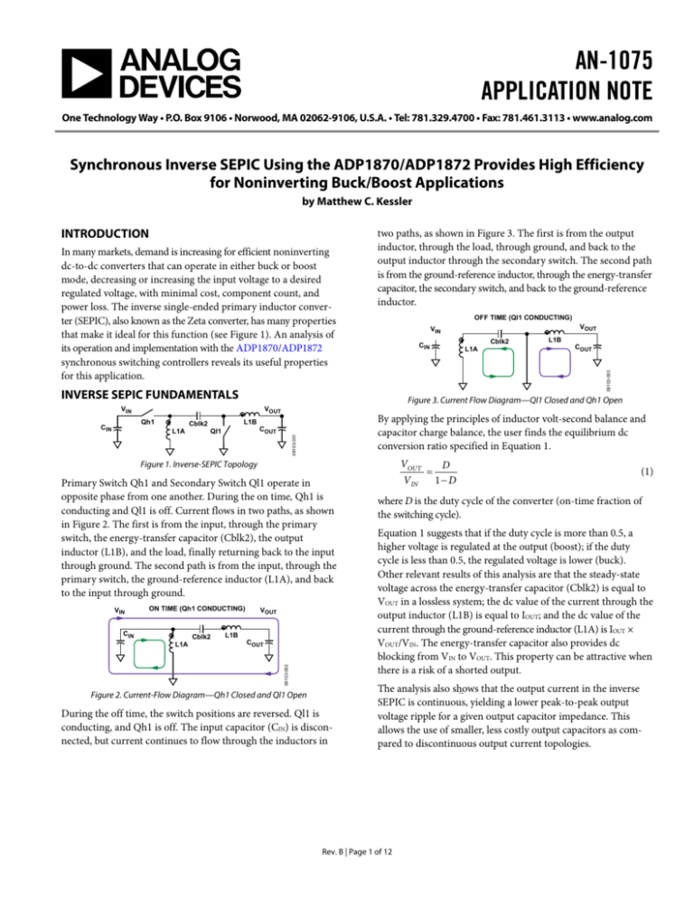
power loss. The inverse single-ended primary inductor converter (SEPIC), also known as the Zeta converter, has many properties
that make it ideal for this function (see Figure 1). An analysis of
its operation and implementation with the ADP1870/ADP1872
synchronous switching controllers reveals its useful properties
for this application.
two paths, as shown in Figure 3. The first is from the output
inductor, through the load, through ground, and back to the
output inductor through the secondary switch. The second path
is from the ground-reference inductor, through the energy-transfer
capacitor, the secondary switch, and back to the ground-reference
inductor.
OFF TIME (Ql1 CONDUCTING)
L1A
L1B
COUT
Figure 3. Current Flow Diagram—Ql1 Closed and Qh1 Open
VIN
VOUT
By applying the principles of inductor volt-second balance and
capacitor charge balance, the user finds the equilibrium dc
conversion ratio specified in Equation 1.
L1B
Cblk2
L1A
COUT
QI1
09103-001
Qh1
Figure 1. Inverse-SEPIC Topology
VOUT
Primary Switch Qh1 and Secondary Switch Ql1 operate in
opposite phase from one another. During the on time, Qh1 is
conducting and Ql1 is off. Current flows in two paths, as shown
in Figure 2. The first is from the input, through the primary
switch, the energy-transfer capacitor (Cblk2), the output
inductor (L1B), and the load, finally returning back to the input
through ground. The second path is from the input, through the
primary switch, the ground-reference inductor (L1A), and back
to the input through ground.
VIN
VIN
Cblk2
CIN
INVERSE SEPIC FUNDAMENTALS
CIN
VOUT
VIN
09103-003
INTRODUCTION
ON TIME (Qh1 CONDUCTING)
CIN
Cblk2
L1B
COUT
09103-002
L1A
VOUT
Figure 2. Current-Flow Diagram—Qh1 Closed and Ql1 Open
=
D
1− D
(1)
where D is the duty cycle of the converter (on-time fraction of
the switching cycle).
Equation 1 suggests that if the duty cycle is more than 0.5, a
higher voltage is regulated at the output (boost); if the duty
cycle is less than 0.5, the regulated voltage is lower (buck).
Other relevant results of this analysis are that the steady-state
voltage across the energy-transfer capacitor (Cblk2) is equal to
VOUT in a lossless system; the dc value of the current through the
output inductor (L1B) is equal to IOUT; and the dc value of the
current through the ground-reference inductor (L1A) is IOUT ×
VOUT/VIN. The energy-transfer capacitor also provides dc
blocking from VIN to VOUT. This property can be attractive when
there is a risk of a shorted output.
The analysis also shows that the output current in the inverse
SEPIC is continuous, yielding a lower peak-to-peak output
voltage ripple for a given output capacitor impedance. This
allows the use of smaller, less costly output capacitors as compared to discontinuous output current topologies.
V out
V in
During the off time, the switch positions are reversed. Ql1 is
conducting, and Qh1 is off. The input capacitor (CIN) is disconnected, but current continues to flow through the inductors in
Rev. B | Page 1 of 12
⎛ D ⎞
⎟
= ⎜⎜
⎟
⎝ (1 − D )⎠
AN-1075
Application Note
TABLE OF CONTENTS
Introduction ...................................................................................... 1 Capacitively Coupled Gate Drive Circuit ..................................5 Inverse SEPIC Fundamentals.......................................................... 1 Small-Signal Analysis and Loop Compensation.......................5 Revision History ............................................................................... 2 Power Component Stresses..........................................................6 Inverse SEPIC Topology Implemented with the
ADP1870/ADP1872 ......................................................................... 3 Lab Results .....................................................................................7 Conclusion..........................................................................................9 Synchronous Implementation .................................................... 3 References.......................................................................................9 Predicting Switching Frequency................................................. 4 Appendix A ..................................................................................... 10 Inductor Coupling, Energy-Transfer Capacitor....................... 4 REVISION HISTORY
9/10—Rev. A: Rev. B
Changes to Inductor Coupling, Energy-Transfer Capacitor
Section................................................................................................ 5
Changes to Power Component Stresses Section........................... 6
7/10—Rev. 0: Rev. A
Changes to Figure 9, Figure 10, and Figure 11 ............................. 7
6/10—Revision 0: Initial Version
Rev. B | Page 2 of 12
Application Note
AN-1075
INVERSE SEPIC TOPOLOGY IMPLEMENTED WITH THE ADP1870/ADP1872
threshold during the off time when the Node X voltage is
approximately equal to −VOUT.
SYNCHRONOUS IMPLEMENTATION
Typically, the secondary switch (Ql1) is a unidirectional power
diode, which limits the peak efficiency of this topology. However, with the Analog Devices, Inc., ADP1870/ADP1872 singlechannel synchronous switching controllers (see Appendix A),
an inverse SEPIC can be designed in a fully synchronous
configuration, employing a bidirectional MOSFET as the
secondary switch. This allows the peak efficiency to increase
considerably, while decreasing the size and cost of the converter
at output currents greater than approximately 500 mA.
The ADP1871 and ADP1873 are members of the ADP187x family
that have a pulse-skip mode (PSM) that increases the efficiency at
light loads by decreasing the switching rate, delivering just
enough energy to the output to keep the output voltage in regulation, considerably decreasing the gate charge and switching loss
in the buck topology. It is not recommended to implement the
ADP1871 and ADP1873 in the synchronous inverse SEPIC
topology.
Figure 5 shows the power stage of the fully synchronous inverse
SEPIC configuration, as implemented with the ADP1870/
ADP1872. The implementation requires only three small,
inexpensive additional components (Cblk1, Ddrv, and Rdrv)
that dissipate negligible power.
VIN + VOUT
SW NODE
NODE X
VIN
0V
The ideal steady-state waveforms of the inverse SEPIC are shown
in Figure 4. The switch node, SW, (see Figure 5) is toggled
between (VIN + VOUT) during the on time and 0 V during the off
time. Connecting Charge-Pump Capacitor Cbst to SW imposes
a voltage that is approximately equal to VIN + VOUT + VDD on the
bootstrapped upper rail of the high-side internal driver (BST
pin) and the output of the high-side driver (DRVH pin) during
the on time, thus enhancing the primary floating N-channel
MOSFET switch, Qh1. The clamping diode, Ddrv, ensures that
Cblk1 has approximately VOUT + VFWD (Ddrv) across it during
steady-state, as referenced from the DRVH pin to the gate of
Qh1, by effectively putting Cblk1 and Cblk2 in parallel during
the off time. The voltage across Cblk1 keeps the primary switch
from developing a gate-to-source voltage that is higher than its
t
–VOUT
IOUT
IOUT × D/(1 – D)
L1A
t
ON TIME
OFF TIME
Figure 4. Ideal Waveforms of Synchronous Inverse SEPIC,
Dead Time Ignored
VDD/VREG
VIN
VDD/VREG
CIN
Qh1
NODE X
BST
L1A
Cbst
Ddrv
FLOATING
DRIVER
Rdrv
Cblk2
DRVH
DRIVER SIGNAL
Cblk1
ADP1870/ADP1872
L1B
SW
(PARTIALLY SHOWN)
VOUT
SW NODE
COUT
Ql1
GROUND
REFERENCED
DRIVER
09103-013
DRVL
PGND
Figure 5. Power Stage with the ADP1870/ADP1872 Internal Drivers Shown
Rev. B | Page 3 of 12
09103-005
L1B
0A
AN-1075
Application Note
Qh1
CIN
Cblk1
Rdrv
ADP1870/ADP1872
1
L1A
Ddrv
10
VIN
NODE X
Cblk2
BST
CVIN
COMP/EN
CC2
SW
RC
VOUT
SW NODE
U1
CC1
FB
DRVH
GND
PGND
VDD/VREG
DRVL
L1B
COUT
Cbst
6
5
CVDD
VDD
Ql1
ADP1872
RF1
09103-004
RF2
NOTES
1. PIN 5 IS VDD IN THE ADP1872 AND VREG IN THE ADP1870.
Figure 6. Complete Implementation of Synchronous Inverse SEPIC with ADP1870/ADP1872
PREDICTING SWITCHING FREQUENCY
As described in Appendix A, the ADP1870/ADP1872 use a constant on time architecture with feedforward and switch node
averaging techniques to minimize switching frequency variations typically associated with constant on time architectures.
The SW pin is connected to the SW node as implemented in
the synchronous inverse SEPIC topology (see Figure 6). Accordingly, the switching frequency for each of the parts in the
ADP1870/ADP1872 series can be predicted as follows:
1
f SW
V
= a × ( OUT + 1)
VIN
(2)
ADP187xARMZ-0.3-R7 − a = 3.33 × 10⁻⁶
ADP187xARMZ-0.6-R7 − a = 1.66 × 10⁻⁶
ADP187xARMZ-1.0-R7 − a = 1 × 10⁻⁶
It should be noted that although these parts are designated as
300 kHz, 600 kHz, and 1 MHz, respectively, these designations
only apply to the approximate switching frequency when
implemented in the buck topology.
INDUCTOR COUPLING, ENERGY-TRANSFER
CAPACITOR
The L1A and L1B power inductors are shown coupled in Figure 6.
The purpose for coupling the inductors in this topology is to
reduce ripple in the output voltage and inductor current, and to
increase the maximum potential closed-loop bandwidth, as
explained in the Small-Signal Analysis and Loop Compensation
section.
Even though the inductors are coupled, it is undesirable for the
coupling to be tight enough to transfer significant energy from
one winding to the other through the core. This can be avoided
by finding the leakage inductance (LLKG) of the coupled inductor
and sizing the energy-transfer capacitor (Cblk2) such that the
magnitude of its complex impedance is a tenth of the complex
series impedance of the leakage inductance and DCR of a single
winding as designated in Equation 2, Equation 3, and Equation 4.
Designing the circuit to conform to this relationship minimizes
the energy transfer through the coupled core. The leakage inductance can be calculated from the coupling coefficient, commonly
found in coupled inductor data sheets.
As shown in Figure 7, the switch node average is fed into the on
timer. In a lossless system, this average is equal to the output
voltage. As the output load increases and the losses in the converter
increase, the switch node average becomes slightly less representative of the output voltage, resulting in an increase in switching
frequency with an increase in output loading. Typically, this
increase is not greater than 10% of the no load condition across
the full load range of the load. In very lossy systems, the increase in
the switching frequency can be greater than this.
Rev. B | Page 4 of 12
⎛
1
| Z Cblk 2 | = ESR + ⎜⎜
π
2
Cblk
2 f SW
⎝
2
⎞
⎟
⎟
⎠
| Z LLKG | = DCR 2 + (2πL LKG f SW )2
| Z Cblk 2 | ≤
| Z LLKG |
10
2
(3)
(4)
(5)
Application Note
AN-1075
As shown in the current flow diagrams, Figure 2 and Figure 3,
charge is deposited and removed during the on time and off
time, respectively. The current flow through the energy-transfer
capacitor should not cause a voltage deviation greater than
±10% of its nominal dc voltage, VOUT, as derived in the
Synchronous Implementation section. Sizing Cblk2 such that
the following inequality is true ensures that the voltage deviation is sufficiently small.
(VOUT × 0.1) ≥
I OUT D
V D
+ ( IN
+ I OUT )Cblk 2 ESR
fswCblk 2 2L1Bf SW
(6)
When coupling the inductors, a 1:1 turns ratio is necessary and
desirable because it requires half the inductance for each
winding that discrete inductors need for a given level of output
voltage ripple (see “Coupled-Inductor and Other Extensions of
a New Optimum Topology Switching DC-DC Converter” by
Ćuk and Middlebrook in the References section).
CAPACITIVELY COUPLED GATE DRIVE CIRCUIT
f RES =
1
At this frequency, there can be 300° or more of high Q phase
lag. To avoid a low phase margin converter across the full load
range, the designer should target a crossover frequency (fUNITY)
at one-tenth of fRES. Dampening of this resonance is largely
dependent on the output loading resistance and the coupled dc
resistance of the inductor. To a lesser extent, dampening is
dependent on the equivalent series resistance (ESR) of the
energy-transfer capacitor, and the on resistance of the power
MOSFETs (Qh1 and Ql1). Therefore, as the output load
resistance varies, the signature of the closed-loop transfer
function may change dramatically at this frequency.
The coupling coefficient is often not a well-controlled parameter,
so the target crossover frequency, fUNITY, should be set to a
decade below fRES, assuming that fRES is less than the switching
frequency, fSW. Standard Type II compensation, with two poles
and a zero, can be used when fUNITY is set appropriately.
F
The value of the gate drive capacitor, Cblk1, is bounded by
several operating parameters. It should be of sufficiently high
capacitance that the deposition and removal of charge during
the turn on and turn off, respectively, of the high-side switch do
not cause the voltage to deviate more than ±10% from its
nominal dc value. This dc value is VOUT + VFWD (Ddrv), as
mentioned in the Synchronous Implementation section. The
value of Cblk1 should also be a tenth of Cbst to avoid excessive
BST-to-SW node voltage during fault conditions. Finally, the
RC time constant of Cbst and Rdrv should be significantly
longer than the switching period. Rdrv provides a discharge
path for Qh1 after the converter is disabled. Good starting
values for Cblk1 and Rdrv are 100 nF and 1 kΩ, respectively.
Correspondingly, Cbst should be 1 μF. A common, small, and
inexpensive BAT54 Schottky barrier diode is sufficient for Ddrv
because it conducts very little current.
f ⎞
⎛f
f UNITY = Minimum⎜ RES , SW ⎟
⎝ 10 10 ⎠
(8)
The compensation-component values in the lower box can be
calculated as follows:
RC =
2πfUNITY COUT (ESR + RLOAD )2 VOUT
GmGCS RLOAD 2VREF
C C1 =
CC0 =
First, there are many complex impedance interactions at the
resonant frequency (fRES), which must be calculated initially to
find the upper limit on the target crossover frequency. When
the inductors are uncoupled, the resonant frequency decreases,
significantly decreasing the potential maximum closed-loop
bandwidth.
unity
Figure 7 shows the equivalent circuit of the ADP1870/ADP1872
feedback loops when employed in a synchronous inverse SEPIC
buck/boost topology. The upper box contains the power stage
and inner current loop; the lower box contains the voltage
feedback loop and compensation circuitry.
SMALL-SIGNAL ANALYSIS AND LOOP
COMPENSATION
A complete small-signal analysis of the inverse SEPIC converter
is beyond the scope of this application note. However, from an
applications perspective, most of this analysis is unnecessary,
and a robust circuit can be designed by following a few
guidelines.
(7)
2π 2L LKG Cblk2
C OUT (R LOAD + ESR)
RC
CC1 ESR
RLOAD
(9)
(10)
(11)
where:
COUT is the output capacitance of the converter.
ESR is the equivalent series resistance of the output capacitor.
RLOAD is the minimum output load resistance.
Gm is the transconductance of the error amplifier, 520 μs for the
ADP1870/ADP1872 family.
VREF is the reference voltage that is tied to the positive input of
the error amplifier, 0.6 V for the ADP1870/ADP1872.
Rev. B | Page 5 of 12
AN-1075
Application Note
POWER STAGE AND INNER CURRENT LOOP
VIN
VOUT
CIN
L1B
Cblk2
Qh1
COUT
RLOAD
L1A
ESR
Ql1
S Q
R
ACS
tON
TIMER
LPF
VOLTAGE FEEDBACK LOOP AND COMPENSATION
RF1
Gm
VCOMP
CC0
CC1
RF2
VREF
09103-006
RC
Figure 7. Power Stage with Inner Current-Sensing Loop and Compensation Scheme of the ADP1870/ADP1872 Configured in Synchronous Inverse SEPIC Topology
GCS, the transconductance of the converter, is calculated by:
GCS =
1
1 ⎞
ACS R DS(ON ) MIN ⎛⎜
⎟
⎝1− D ⎠
=
ΔI OUT
ΔVCOMP
(12)
where:
GCS is a frequency-independent gain term that varies with
RDS(ON), the resistance of the secondary switch when enhanced,
and duty cycle, D. It is expected that the highest crossover
frequency occurs when this resistance and the duty cycle, D, are
at their lowest.
Acs is the current sense gain, which, with the ADP1870/ADP1872,
is selectable in four discrete steps from 3 V/V to 24 V/V.
To ensure that current limit is not induced prematurely, the
highest value of current-sense gain (ACS) that obeys the following inequality should be selected:
1 ⎞ ΔI L ⎞
⎛
2.53 V ≥ ACS RDS(ON ) MAX ⎜ I OUT ⎛⎜
⎟ + 1.15 V (13)
⎟−
⎝ 1 − D ⎠ 1.2 ⎠
⎝
where ΔIL is the peak-to-peak inductor ripple current.
ΔI L =
VIN D
2L1Bf SW
(14)
Because the ADP1870/ADP1872 use a constant on time
architecture, the sampling poles typically associated with
current mode control are not present in the control loop.
Therefore, the complexity of adding the appropriate amount
of slope compensation to the sensed current signal is not
necessary.
POWER COMPONENT STRESSES
The current-flow diagrams in Figure 2 and Figure 3 show that
the power MOSFETs, when conducting, carry the sum of the
inductor currents. Accordingly, the dc component of the current through both switches is
I DC = I OUT
1
1− D
(15)
The ac component of the current through both switches is
I AC =
VIN D
L1Af SW
(16)
With dc and ac components of the MOSFET current known
(shown in Figure 8), the designer can quickly calculate the rms
values of the current through each switch. In conjunction with
the RDS(ON)MAX of the selected MOSFETs, the rms values can be
used to ensure that the MOSFETs are thermally stable, with power
dissipation low enough to meet the efficiency requirements.
Rev. B | Page 6 of 12
Application Note
AN-1075
LAB RESULTS
IAC
1/fSW
0A
Qh1
Ql1
Cblk2
09103-007
t
Figure 9, Figure 10, and Figure 11 show a comparison of the
efficiencies achieved for a range of input voltages to 5 V out
with both the synchronous inverse SEPIC and asynchronous
SEPIC, a more traditional way of implementing a noninverting
buck boost. Both circuits have been individually optimized for
efficiency to meet a wide input voltage range application and
are provided a low current 5 V bias.
1.00
Figure 8. Ideal Current Waveforms of Synchronous Inverse SEPIC,
Dead Time Ignored
SYNCHRONOUS INVERSE SEPIC
ASYNCHRONOUS SEPIC
EFFICIENCY (%)
0.95
Calculating switching loss in the primary switch accurately is
beyond the scope of this application note, but it should be noted
that, in transitioning from high resistance to low resistance
states, the voltage across the MOSFET swings from ~(VIN + VOUT)
to ~0 V, and the current through the device swings from 0 A to
~IOUT(1/(1 – D)). Switching loss can be the predominant loss
with swings of these magnitudes, a factor the user should be
aware of when selecting a MOSFET for which the reverse transfer
capacitance (CRSS) and RDS(ON) are inversely proportional.
0.90
0.85
0.80
0.75
The drain-source breakdown voltage (BVDSS) for both the primary and secondary switches must be greater than the input
voltage plus the output voltage (see Figure 4).
0.70
The peak-to-peak output-voltage ripple (ΔVRIPPLE) is
approximated by
0.95
ΔI L
+ ΔI L × ESR
8 f SW C OUT
10
15
20
Figure 9. Efficiency vs. Load Current (VIN = 12 V, VOUT = 5 V)
0.90
(17)
ΔI L
2 3
(18)
0.85
0.80
0.75
The peak-to-peak inductor current (ΔIL) designated in Equation 14
depends on the input voltage, so the designer must ensure that,
as this parameter varies, the output-voltage ripple does not
exceed the specification, and the rms current through the
output capacitor does not exceed its rating.
SYNCHRONOUS INVERSE SEPIC
ASYNCHRONOUS SEPIC
0.70
0
2
4
6
8
10
12
LOAD CURRENT (A)
09106-011
The rms value of the current through the output capacitor
(IrmsCout) is
I rmsCout ≈
5
LOAD CURRENT (A)
EFFICIENCY (%)
ΔVRIPPLE ≈
0
09106-010
IDC
Figure 10. Efficiency vs. Load Current (VIN = 5 V, VOUT = 5 V)
As shown in Figure 8, the rms current through the energytransfer capacitor, Cblk2, is
0.95
Irms Cblk 2 =
0.90
2
2
D⎤
D ⎡ ΔI L ⎤
(1 − D) ⎡ ΔI L ⎤
⎡I
+ (1 − D)⎢ OUT ⎥ +
⎢
⎥
⎢
⎥
3⎣ 2 ⎦
3 ⎣ 2 ⎦
⎣ (1 − D) ⎦
For high output current applications, putting multiple
capacitors in parallel for Cblk2 is often necessary to avoid
exceeding the rms rating on an individual capacitor.
For synchronous inverse SEPICs implemented with the ADP1870/
ADP1872, the input voltage plus the output voltage must not
exceed 20 V because the charge-pump capacitor is connected to
the switch node, which reaches VIN + VOUT when the primary
switch is conducting.
Rev. B | Page 7 of 12
0.85
0.80
0.75
SYNCHRONOUS INVERSE SEPIC
ASYNCHRONOUS SEPIC
0.70
0
2
4
6
8
LOAD CURRENT (A)
Figure 11. Efficiency vs. Load Current (VIN = 3.3 V, VOUT = 5 V)
09106-012
D × I OUT 2 +
EFFICIENCY (%)
2
AN-1075
Application Note
The synchronous inverse SEPIC was implemented with the
ADP1872, and the bill of materials for the relevant power
components is shown in Table 1, which includes only common
off-the-shelf components. The asynchronous SEPIC was
implemented with an ADP1621 switching controller from
Analog Devices. The bill of materials for the relevant power
components is shown in Table 2.
As shown in Figure 9 to Figure 11, the synchronous inverse
SEPIC is always more efficient than the asynchronous at any
output current above approximately 500 mA. At each input
voltage, the synchronous inverse SEPIC is capable of providing
more output current, at higher efficiency, and with less components. As described in Table 1 and Table 2, the synchronous
inverse SEPIC uses two MOSFETs for the power conversion,
whereas the asynchronous SEPIC uses two MOSFETs and a
large power diode for the power conversion. This result of this
is a lower part count, smaller footprint, lower cost, and more
output current capability when implemented in the
synchronous configuration.
Table 1. Power Components—Synchronous Inverse SEPIC Implemented with ADP1872
Designator
Part Number
Manufacturer
Value
Package
Comment
Qh1
BSC090N03MS
Infineon
30 BVDDS
SuperSO8
Ql1
BSC016N03MS
Infineon
30 BVDDS
SuperSO8
L1A/L1B
PCA20EFD-U10S002
TDK
3.4 μH per
winding
30 mm × 22 mm ×
12 mm
Power MOSFET, 11.2 mΩ (maximum) at 4.5 VGS,
TJ = 25°C
Power MOSFET, 2 mΩ (maximum) at 4.5 VGS,
TJ = 25°C
1:1:1:1:1:1 coupled inductor, ferrite, 35.8 mΩ
(maximum) DCR per winding
Table 2. Power Components—Asynchronous SEPIC Implemented with ADP1621
Designator
Part Number
Manufacturer
Value
Package
Comment
Power MOSFET
BSC057N03MS
Infineon
30 BVDDS
SuperSO8
Power Diode
Coupled Inductor
PDS1040L
DRQ127-2R2-R
Diodes Inc.
Cooper Bussmann
40 BVRRM/10 IO
2.03 μH per
winding
PowerDI5
10 mm × 12.5 mm ×
8 mm
Quantity = 2, 7.2 mΩ (maximum) at 4.5 VGS,
TJ = 25°C
VF = 0.46 V (maximum) at TS = 25°C
1:1 coupled inductor, ferrite, 7 mΩ
(maximum) DCR per winding
Rev. B | Page 8 of 12
Application Note
AN-1075
CONCLUSION
The need for high efficiency noninverting dc-to-dc converters
that provide both higher and lower voltages than the input (boost
and buck) is increasing in many markets. The Analog Devices
ADP1870/ADP1872 single-phase synchronous switching
controllers allow the high loss power diode commonly used in
the power stage to be replaced by a low loss MOSFET. With this
increase in efficiency comes a cost and solution size reduction
that allows the system to meet stringent energy requirements.
Robust compensation component values can be calculated
quickly by following a few guidelines, and high efficiency can
be achieved with common off-the-shelf components.
REFERENCES
Ćuk, Slobodan and R.D. Middlebrook. 1983. “CoupledInductor and Other Extensions of a New Optimum Topology
Switching DC-DC Converter.” Advances in Switched-Mode
Power Conversion, Volumes I and II. Irvine, CA: Tesla Co.
Rev. B | Page 9 of 12
AN-1075
Application Note
APPENDIX A
has an internal linear regulator, whereas the ADP1872 requires
a 2.75 V to 5.5 V bias supply.
The ADP1870/ADP1872, shown in Figure 12, are constant on
time switching controllers with integrated drivers that drive Nchannel synchronous power MOSFETs. The constant on time
architecture uses input voltage feedforward and switch node
averaging techniques to reduce switching frequency variation
typically associated with constant on time architectures. The
family also uses a leading edge modulation valley current mode
control scheme.
The ADP1870/ADP1872 include an internally set soft start
period, hiccup mode current limit, thermal shutdown protection, and are available in three different switching frequencies.
The ADP1870/ADP1872 provide an output voltage accuracy of
−0.834%/+0.884% from –40°C to +85°C and −0.834%/+1.084%
from −40°C to +125°C junction temperature. Powered by a 2.75 V
to 20 V power stage input supply, the ADP1870/ADP1872 are
available in the 10-lead MSOP package.
The boost diode is built into the ADP1870/ADP1872, lowering
the overall component count and system cost. The ADP1870
LDO
(ADP1870 ONLY)
COMP/EN
TO ENABLE
ALL BLOCKS
ENABLE BLOCK
tON
BIAS
BLOCK
VREG (ADP1870),
VDD (ADP1872)
VIN
FILTER
VDD
VDD
BST
ISS
DRVH
SS
COMP
SS_REF
DRIVERS
ERROR
AMP
SW
300kΩ
STATE
MACHINE
CSS
DRVL
8kΩ
FB
0.6V
PGND
PWM
VREG
REF_ZERO
800kΩ
CS
AMP
CS GAIN SET
ADC
CS GAIN
PROGRAMMING
GND
Figure 12. ADP1870/ADP1872 Simplified Block Diagram
Rev. B | Page 10 of 12
09103-009
LOWER
COMP
CLAMP
Application Note
AN-1075
NOTES
Rev. B | Page 11 of 12
AN-1075
Application Note
NOTES
©2010 Analog Devices, Inc. All rights reserved. Trademarks and
registered trademarks are the property of their respective owners.
AN09103-0-9/10(B)
Rev. B | Page 12 of 12
