Whites, EE 382
Lecture 15
Page 1 of 6
Lecture 15: Pulse Propagation on TLs.
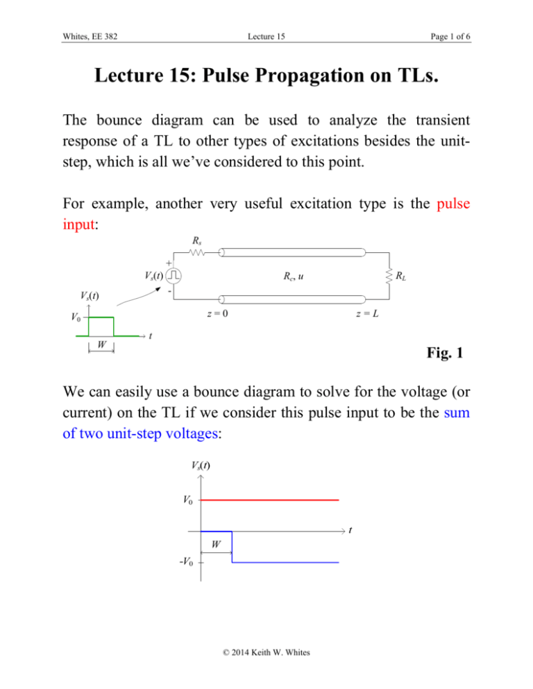
The bounce diagram can be used to analyze the transient
response of a TL to other types of excitations besides the unitstep, which is all we’ve considered to this point.
For example, another very useful excitation type is the pulse
input:
Rs
+
Vs(t)
Rc, u
-
Vs(t)
z=0
V0
W
RL
z=L
t
Fig. 1
We can easily use a bounce diagram to solve for the voltage (or
current) on the TL if we consider this pulse input to be the sum
of two unit-step voltages:
© 2014 Keith W. Whites
Whites, EE 382
Lecture 15
Page 2 of 6
The sum of these two unit-step voltages gives the pulse shown
in Fig. 1.
Use Bounce Diagram for V(z,t) vs. t at a Fixed z
IL(t)
Rs
+
+
s
Vs(t)
L VL(t)
Rc, u
-
RL
z = z0
z=0
W
tL
z=L
z
1
V
1
V
t1
t2
t3
t4
P1
P2
P3
P4
LV1
LV1
2tL
s LV1
3tL
z
t5
t6
t7
t8
s LV1
2L sV1
P5
P6
P7
P8
2L sV1
4tL
2s 2LV1
t9
5tL t10
t11
t12
2s 2LV1
3L 2sV1
P9
P10
P11
P12
3L 2sV1
t
Fig. 2
To use the bounce diagram in this situation:
(i.) Pick a position z0 at which to plot V z0 , t versus time.
Whites, EE 382
(ii.)
Lecture 15
Page 3 of 6
Draw a vertical line at z0 . It intersects the sloping lines at
points P1 through P12 above.
(iii.) At each of these intersection points, draw horizontal lines
and label these times t1 through t12. These are the times at
which new wave fronts arrive and abruptly change the
voltage at z0 .
(iv.) The voltage at z0 versus time is then:
Time range
0 t1
t1 t2
t2 t3
t3 t4
t4 t5
t5 t6
t6 t7
t7 t8
t8 t9
t9 t10
t10 t11
t11 t12
Voltage
0
V1
V1 V1 0
V1 V1 LV1 LV1
V1 V1 LV1 LV1 0
s LV1
0
2L sV1
0
2s 2LV1
0
3L 2sV1
etc…
Depending on the width of the input pulse, these voltages will be
different, as we’ll see in the next example.
Whites, EE 382
Lecture 15
Page 4 of 6
Example N15.1: Imagine that a high speed digital logic gate
(modeled by a pulse voltage source of amplitude 1 V, pulse
width of 200 ps, and output resistance 900 ) drives a load of 25
through a 100- microstrip line ( u 200 m/s) that is 8 cm
long. Sketch the voltage at the load V L, t from 0 to 2.2 ns.
We can model this interconnection problem using a transmission
line as shown:
s
L
For this TL,
L
8 cm
R Rc 900 100
tL
400 ps, s s
0.8 ,
Rs Rc 900 100
u 200 m μs
R Rc 25 100
L L
0.6
and
RL Rc 25 100
At time t = 0+, draw the equivalent lumped-element circuit at the
input to the TL:
Rs=900
1V
Rc
+
V(z=0,t=0+)
-
z=0
Whites, EE 382
Lecture 15
Page 5 of 6
By voltage division in this circuit
Rc
100
1
Vs
1
V
V1
100 900
10
Rc Rs
The pulse width W = 200 ps is less than the one-wave transit
time tL, so the bounce diagram in Fig. 2 is applicable, though it’s
not drawn to precisely represent this specific problem.
We are requested to plot V z L, t . For z0 L , since we’re
looking at the load end, then referring to the bounce diagram in
Fig. 2:
P1 P3
P2 P4
P5 P7
P6 P8
0 t1 t L 400 ps :
VL 0 V
t1 400 ps t2 t L W 600 ps :
1
1
0.6 0.04 V
10
10
t2 600 ps t5 3t L 1200 ps :
VL V1 LV1
VL 0 V
t5 1200 ps t6 3t L W 1400 ps :
Whites, EE 382
Lecture 15
Page 6 of 6
VL s LV1 2L sV1
1
1
2
0.6 0.8 0.0192 V
10
10
t6 1400 ps t9 5t L 2000 ps :
0.8 0.6
VL 0 V
t9 2000 ps t10 5t L W 2200 ps :
VL 2s 2LV1 3L 2sV1
0.82 0.6
2
1
1
3
0.6 0.82 0.00922 V
10
10
Sketch of the output voltage versus time:
VL [V]
0.04
0.04
0.03
0.02
0.01
0.00922
0.4 0.6
-0.01
-0.02
-0.03
-0.04
0.5
1.2 1.4
1
1.5
-0.0192
2
2.2
t (ns)
Propagation of Voltage Pulse and Ramp Waveforms on a Transmission Line
Page 1 of 8
Example 7.3
Propagation of Voltage Pulse and Ramp
Waveforms on a Transmission Line
Purpose
To compute and visualize the propagation of voltage waves on a transmission line. Two
different source voltage waveforms – the pulse and the ramp – will be used in this
worksheet. The computation of the voltage on the TL is accomplished using a numerical
solution called the finite difference time domain method. (Requires Mathcad 8 Professional,
Academic or Explorer.)
Background
A coaxial-cable transmission line is used in this problem as shown in Fig. 7.15a of the text. The
transmission line (TL) model of this coax is depicted in the figure below:
L
RS
+
+
VS
V(z,t)
_
_
Rc
u
z=0
RL
z=L
Although the load resistance was specified as zero in Example 7.3, in this worksheet we will
allow for a nonzero load resistance so that you can investigate other problems of this type that
may have a nonzero load resistance.
Two different types of transient voltage excitation are examined in Example 7.3. Both of these
will be implemented in this worksheet. The propagation of the transient voltage on this TL will
be computed using the FDTD method as described in the Example 7.2 worksheet.
Enter the transmission line, voltage source and FDTD parameters
Choose the parameters for the transmission line (TL):
L := 400
Length of TL (m).
− 12
ctl := 100⋅ 10
Visual Electromagnetics for Mathcad
Per-unit-length capacitance of TL (F/m).
© 2007 by Keith W. Whites.
All rights reserved.
Propagation of Voltage Pulse and Ramp Waveforms on a Transmission Line
−6
ltl := 0.25⋅ 10
Per-unit-length inductance of TL (H/m).
RL := 0
Load resistance (Ω).
Page 2 of 8
For this choice of the per-unit-length capacitance and inductance, the propagation velocity, u,
and characteristic resistance, RC, of the TL are:
u :=
1
8
ltl⋅ ctl
ltl
RC :=
ctl
u = 2 × 10
(m/s)
RC = 50.000
(Ω)
Now choose the source voltage amplitude and the pulse width (i.e., the length of time for
which the source voltage is nonzero):
V0 := 100
Source voltage amplitude (V).
RS := 150
Source resistance (Ω).
−6
W := 6⋅ 10
Pulse width of the source voltage (s).
For the numerical FDTD solution of the voltage on this transmission line, choose the number
of segments in which to subdivide the TL, nz, and the number of time steps to compute the
solution, nt:
nz := 40
Number of segments to subdivide the TL.
nt := 360
Number of time steps to compute the solution.
Compute the uniform spacing of the voltage nodes, Δz, and the time increment Δt:
Δz :=
L
nz
Δt :=
Δz
u
The source voltage pulse is assumed to begin at time t = 0. For nt = 360 time steps, the
final time for which a voltage solution will be computed is:
tend := nt⋅ Δt
−5
tend = 1.800 × 10
(s)
Plot the open-circuit source voltage for the pulse and ramp waveforms
We will first plot the pulse and ramp source voltages to better appreciate these two types of
open-circuit waveforms that we will use in this worksheet. Here we define the program
structure VS(Vt,t) that is used to compute the open-circuit source voltage at any time t:
Visual Electromagnetics for Mathcad
© 2007 by Keith W. Whites.
All rights reserved.
Propagation of Voltage Pulse and Ramp Waveforms on a Transmission Line
VS ( Vt , t) :=
⎛
⎝
V0 − ⎜ Vt −
Page 3 of 8
Vt ⎞
⋅ t⎟ if 0 < t ≤ W
W ⎠
0 otherwise
This source voltage definition is capable of computing both the pulse and ramp shapes used in
Example 7.3 of the text. VS is defined here as the difference between two waveforms: a pulse
of amplitude V0 and a linearly decreasing voltage (in time) that has amplitude Vt at t = 0 and
an amplitude of 0 at t = W. If the desired voltage source is to have a pulse shape, then Vt
should be input as 0. If the desired source is to be an increasing ramp (in time), then Vt should
be input as V0.
Choose the number of points to plot the source waveforms and a set of times tp at which to
plot them:
Number of time points to plot the source voltage.
npts := 150
tp_end := 2⋅ W
Ending time for the plot (s).
i := 0 .. npts − 1
tp := i⋅
i
tp_end
npts − 1
The pulse and ramp voltage sources are shown as a function of time below:
The pulse and ramp source voltages.
6
Open circuit source voltage (V)
100
V0
W⋅ 10
For source
voltages with (V)
V0 = 100
and (s)
50
−6
W = 6 × 10
0
0
2
4
6
8
10
0
12
time (microseconds)
Pulse voltage source
Ramp voltage source
These two open-circuit source voltages will be identical to those indicated in Figs. 7.15b
and 7.15d of the text if V0 = 100 V and W = 6 μs.
Define the FDTD function to compute the TL voltage
Visual Electromagnetics for Mathcad
© 2007 by Keith W. Whites.
All rights reserved.
Propagation of Voltage Pulse and Ramp Waveforms on a Transmission Line
Page 4 of 8
Using the parameters for the TL, the number of segments (nz) and the number of time steps
(nt) for the FDTD solution entered earlier in this worksheet, we can now solve for the voltage
at each node on the TL at each time step. The program structure FDTD given in the following
referenced worksheet
Reference:D:\Classes\EE 382 - Applied Electromagnetics\Lecture notes, EE 382\EE 382, Lecture notes, Mathcad wor
will compute the voltage on the TL once a voltage source waveform (either pulse or ramp) has
been specified.
The voltage on the TL produced by each of these two sources will now be separately
examined in the following four sections of this worksheet.
Pulse voltage source
We will first observe the voltage produced on the TL by a pulse source voltage.
Solve for the voltage at all nz+1 nodes on the TL at all times nt with a pulse voltage source
excitation:
V := FDTD ( 0 , nz , nt)
With the voltages determined at all of the nodes on the TL at the discrete list of times, we will
now generate two plots in order to visualize these results. The first plot is the voltage at the
input to the TL (z = 0) as a function of time.
Voltage at the TL input (z = 0).
Voltage (V)
20
For a pulse
voltage source.
0
20
0
5
10
15
t (microseconds)
Such a plot was also constructed in Example 7.3 of the text by other means. Using the same
source and TL parameters as given in that example, you will observe that the plot shown
above will be identical to that given by the solid line in Fig. 7.15c.
The voltage levels in the above plot can be measured directly from the plot using
the Trace command.
Visual Electromagnetics for Mathcad
© 2007 by Keith W. Whites.
All rights reserved.
Propagation of Voltage Pulse and Ramp Waveforms on a Transmission Line
Page 5 of 8
Pulse voltage source: Animated plot of V propagating on the TL
The next plot we will generate is an animation clip for the voltage on the TL as a
function of time for this pulse voltage source.
The voltage was computed at nt = 360 time steps. Due to the time it takes to construct
the animation of this voltage disturbance on the TL, you may not wish to have Mathcad
construct the animation clip using all of these time steps. Therefore, you can choose the
parameter nskip to specify how many time steps to disregard between successive frames
when generating the animation clip. For example, if nskip = 0, all time steps are used; if
nskip = 1, every second time step is used; if n skip = 2, every third time is used, etc.
nskip := 2
Choose the number of time steps to skip between successive frames
in the animation clip.
Compute the z position of all voltage nodes in the FDTD solution and define the
parameter time in terms of FRAME:
k := 1 .. nz + 1
zk := ( k − 1) ⋅
L
nz
time :=
FRAME⋅ ( nskip + 1) ⋅ Δt
−6
10
Now generate an animation clip of the voltage on this TL. For best results,
in the "Animate" dialog box choose To = 120 .
Voltage on the TL (pulse source).
Voltage (V)
20
At time (μs)
time = 0.000
0
For a TL with
L = 400 (m)
8
u = 2 × 10 (m
/s)
20
0
100
200
300
400
z (meters)
The source is located at the left-hand edge of this plot and the load is located at the right-hand
edge.
One particularly useful application of this animation is to observe the voltage at the input to the
TL as a function of time and compare this voltage to that shown in Fig. 7.15(c) in the text (and
also in the previous plot). You can use the slider bar in the animation viewer to observe this
animation at a desired time instant.
Visual Electromagnetics for Mathcad
© 2007 by Keith W. Whites.
All rights reserved.
Propagation of Voltage Pulse and Ramp Waveforms on a Transmission Line
Page 6 of 8
Performing this comparison, in addition to the analysis technique in Example 7.3, is very helpful
in appreciating how this input voltage varies as a function of time.
Ramp voltage source
Now we will consider the ramp voltage source excitation as shown earlier in this worksheet.
The numerical solution is the same as in the previous pulse example, except now the FDTD
program is called with the source parameter V 0 in the first argument below. As discussed
earlier, this will cause the voltage source to be the ramp excitation:
V := FDTD ( V0 , nz , nt)
With the voltages determined at all of the nodes on the TL at the discrete list of times, we will
now generate two plots in order to visualize these results. The first plot we will generate is the
voltage at the input to the TL (z = 0) as a function of time:
Voltage at the TL input (z = 0).
Voltage (V)
20
For a ramp
voltage source.
0
20
0
5
10
15
t (microseconds)
Using the same source and TL parameters as given in Example 7.3, you will observe that the
plot shown above will be identical to that given by the solid line in Fig. 7.15d.
The voltage levels in the above plot can be measured directly from the plot using
the Trace command.
Ramp voltage source: Animated plot of V propagating on the TL
The final plot we will generate is an animation clip of the voltage on the TL as a function of time
for this ramp voltage source. First choose the parameter nskip. As described earlier in this
worksheet, if nskip = 0, all time steps are used; if nskip = 1, every second time step is used; if
nskip = 2, every third time is used, etc., in the generation of the animation clip:
Visual Electromagnetics for Mathcad
© 2007 by Keith W. Whites.
All rights reserved.
Propagation of Voltage Pulse and Ramp Waveforms on a Transmission Line
nskip := 2
Page 7 of 8
Choose the number of time steps to skip between successive frames
in the animation clip.
Compute the z position of all voltage nodes in the FDTD solution and define the parameter
time in terms of FRAME:
time :=
FRAME⋅ ( nskip + 1) ⋅ Δt
−6
10
Now generate an animation clip of the voltage on this TL. For best results,
in the "Animate" dialog box choose To = 120 .
Voltage on the TL (ramp source).
Voltage (V)
At time (μs)
time = 0.000
0
For a TL with
L = 400 (m)
8
u = 2 × 10 (m
/s)
20
0
100
200
300
400
z (meters)
It is interesting to observe in this animation that the voltage waveform that initially propagates
along this TL has the sloped edge pointing towards the right whereas the plot of this ramp
waveform shown earlier in this worksheet (and in Fig. 7.15d of the text) has the sloped edge of
the voltage on the left. This behavior is due to the fact that the latter plot is the open-circuit
source voltage as a function of time, whereas the former plot (i.e., the animation clip above) is
the voltage as a function of position (and time) along the TL. In fact, as is discussed in the text
following Example 7.3, the voltage waveform we initially observe in this animation clip appears
as a "flipped around" version of the open-circuit source voltage. This occurs because the
linearly increasing portion of the ramp source is the first to excite the TL and, consequently, the
first to begin propagation along the TL. We did not observed this behavior with the pulse input
earlier in this worksheet since the leading and trailing edges of this waveform look identical.
You may wish to experiment with other waveforms to more clearly see this behavior. For
example, choosing a smaller width for the source, such as W = 10 -6 (1 μs) will give a ramp (or
pulse) waveform that is much smaller than the one-way transient time on the TL using the
parameters for the TL given in Example 7.3. When you generate the animation clip for this
case, look for the total reflection of the voltage waveform at the load which will cause the
incident ramp to undergo an inversion as it propagates back towards the source.
Visual Electromagnetics for Mathcad
© 2007 by Keith W. Whites.
All rights reserved.
Propagation of Voltage Pulse and Ramp Waveforms on a Transmission Line
Page 8 of 8
End of worksheet.
Visual Electromagnetics for Mathcad
© 2007 by Keith W. Whites.
All rights reserved.


