Technical Article
MS-2275
.
Common Inter-IC Digital
Interfaces for Audio Data
Transfer
but now digital interfaces are being included on the
transducers and amplifiers that usually have had only analog
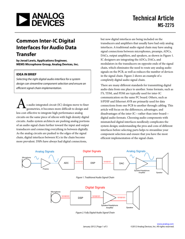
interfaces. A traditional audio signal chain may have analog
signal connections between microphones, preamps, ADCs,
DACs, output amplifiers, and speakers, as shown in Figure 1.
IC designers are integrating the ADCs, DACs, and
modulators in the transducers on opposite ends of the signal
chain, which eliminates the need to route any analog audio
signals on the PCB, as well as reduces the number of devices
in the signal chain. Figure 2 shows an example of a
completely digital audio signal chain.
by Jerad Lewis, Applications Engineer,
MEMS Microphone Group, Analog Devices, Inc.
IDEA IN BRIEF
Selecting the right digital audio interface for a system
design can streamline component selection and ensure an
There are many different standards for transmitting digital
audio data from one place to another. Some formats, such as
I2S, TDM, and PDM are typically used for inter-IC
communication on the same PC board. Others, such as
S/PDIF and Ethernet AVB are primarily used for data
connections from one PCB to another through cabling. This
article will focus on the differences, advantages, and
disadvantages of the inter-IC—rather than inter-board—
digital audio formats. Choosing audio components with
mismatched digital interfaces needlessly complicates the
system design; understanding the pros and cons of different
interfaces before selecting parts helps to streamline your
component selection and ensure that you have the most
efficient implementation of the signal chain.
efficient signal chain implementation.
A
s audio integrated circuit (IC) designs move to finer
geometries, it becomes more difficult to design and
less cost-effective to integrate high performance analog
circuits on the same piece of silicon with high density digital
circuits. Audio system architects are pushing analog portions
of an audio signal chain further toward the input and output
transducers and connecting everything in between digitally.
As the analog circuits are pushed to the edges of the signal
chain, digital interfaces between ICs in the chain become
more prevalent. DSPs have always had digital connections,
Digital Signals
Analog Signals
Analog Signals
Microphone
ADC
10100101
DSP
10100101
DAC
Preamp
Speaker/Headphone
Amplifier
Speaker
Figure 1. Traditional Audio Signal Chain
Digital Signals
Microphone
10100101
DSP
10100101
10100101
Speaker/Headphone
Amplifier
Speaker
Figure 2. Fully Digital Audio Signal Chain
January 2012 | Page 1 of 3
www.analog.com
©2012 Analog Devices, Inc. All rights reserved.
MS-2275
Technical Article
Inter-IC Sound (more commonly called “I-squared-S” or “Itwo-S”) is the most common digital audio format used for
audio data transfer between ICs. The I2S standard was
introduced by Philips Semiconductors (now NXP) in 1986
and was revised in 1996. The interface was first popularlyused in CD player designs, and now can be found in almost
any application where digital audio data is being transferred
from one IC to another. Most audio ADCs, DACs, DSPs, and
sample rate converters, and some microcontrollers, include
I2S interfaces.
An I2S bus uses three signal lines for data transfer: a frame
clock, a bit clock, and a data line. The two clocks can be
generated by the receiving IC, the transmitting IC, or even a
separate clock master IC, depending on the system
architecture. An IC with an I2S port can often be set to be in
either master or slave mode. Unless a sample rate converter
is being used in the signal chain, a system will usually have a
single I2S master device so that there are no issues with data
synchronization.
I S Source
2
Modulator &
Decimation
Filter
Bit Clock
Frame Clock
Serial Data Output
I2S Receiver
(Processor, codec)
Bit Clock
Frame Clock
Clock
Generator
Serial Data Input
Figure 3. I2S Connection Diagram, Receiver as Master
The Philips standard for these signals uses the names WS for
word select, SCK for the clock, and SD for the data, although
IC manufacturers seem to rarely use these names in their IC
data sheets. Word select is also commonly called LRCLK, for
“left/right clock,” and SCK may be called BCLK, for “bit
clock” or SCLK for “serial clock.” The name of an IC’s serial
data pin varies most from one IC vendor to another, and
even within a single vendor’s different products. A quick
survey of audio IC data sheets shows that the SD signal may
also be called SDATA, SDIN, SDOUT, DACDAT, ADCDAT,
or other variations on these, depending on whether the data
pin is an input or output.
An I2S data stream can carry one or two channels of data
with a typical bit clock rate between 512 kHz, for an 8 kHz
sampling rate, and 12.288 MHz, for a 192 kHz sampling rate.
The data word length is often 16, 24, or 32 bits. For word
www.analog.com
©2012 Analog Devices, Inc. All rights reserved.
lengths less than 32 bits, the frame length is often still 64 bits
and the unused bits are just driven low by the transmitting
IC. Although it is rare, some ICs only support I2S interfaces
with a maximum of 32 or 48 bit clocks per stereo audio
frame. A system designer has to be careful when using one of
these ICs to make sure that the devices on the other end of
its connections can also support these bit clock rates.
While I2S format is the most commonly used, there are other
variants of this same 3-wire configuration, such as leftjustified, right-justified, and PCM modes. These differ from
I2S by the position of the data word in the frame, the polarity
of the clocks, or the number of bit clock cycles in each
frame.
Some ICs support multiple I2S data inputs or outputs using a
common clock, but this obviously increases the number of
pins necessary to transfer the data. Time division
multiplexed (TDM) formats are used when more than two
channels of data are to be transferred on a single data line. A
TDM data stream can carry as many as sixteen channels of
data and has a data/clock configuration similar to that of I2S.
Each channel of data uses a slot on the data bus that is 1/Nth
the width of the frame, where N is the number of channels
being transferred. For practical purposes, N is usually
rounded up to the nearest power-of-two (2, 4, 8, or 16) and
any additional channels are left empty. A TDM frame clock is
often implemented as a single bit-wide pulse, rather than
I2S’s 50% duty cycle clock. Clock rates above 25 MHz are not
commonly used for TDM data, since higher frequencies
cause board layout issues that PCB designers would rather
avoid.
TDM is commonly used for a system with multiple sources
feeding one input, or one source driving multiple devices. In
the former case, each TDM source shares a common data
bus. The source must be configured to drive the bus only
during its appropriate channel, and tri-state its driver while
the other devices are driving the other channels.
There is no standard for TDM interfaces, such as the Philips
standard for I2S. This means that many ICs have their own
slightly-different flavor of a TDM implementation. These
differences may include clock polarities, channel
configuration, and tri-stating or driving unused channels. Of
course, these different ICs will usually work together, but a
system designer needs to take care to ensure that outputs of
one device will spit out data in the format that the inputs of
another are expecting!
January 2012 | Page 2 of 3
Technical Article
MS-2275
PDM data connections are becoming more common in
portable audio applications, such as cell phones and tablet
computers. This is an advantage in these size-constrained
applications because PDM audio signals can be routed
around noisy circuitry, such as LCD screens, without having
to deal with interference issues analog audio signals might
have. With PDM, up to two audio channels can be
transmitted with only two signal lines. Figure 4 shows a
system diagram with two PDM sources driving a common
data line into a receiver. A clock generated by the system
master can be used by two slave devices, which use alternate
edges of the clock to output their data on a common signal
line. The data is modulated at a 64× rate, resulting in a clock
that is typically between 1.0 MHz and 3.2 MHz. The
bandwidth of the audio signal increases as the clock rate
increases, so lower frequency clocks are used in systems
where a reduced bandwidth can be traded off for lower
power consumption.
PDM Source 1
Modulator
Clock
Data Output
PDM Receiver
(Processor, codec, amplifier)
Clock
PDM Source 2
Modulator
Data Input
Decimation
Filter &
Clock
Generator
Clock
Data Output
Figure 4. Dual-Source PDM Connection Diagram
A PDM-based architecture differs from I2S and TDM in that
the decimation filter is in the receiving IC, rather than the
transmitting IC. The output of the source is the raw high
sample rate modulated data, such as the output of a SigmaDelta modulator, rather than a decimated data, as it is in I2S.
A PDM-based architecture reduces the complexity in the
source device, and often makes use of decimation filters that
are already present in a codec’s ADCs. This allows system
designers to use audio codecs that they may already be
using, but take advantage of a digital data connection’s
reduced sensitivity to interference. Also, these decimation
filters may be more efficiently implemented in the finer
silicon geometries used for fabricating a codec or processor,
rather than what is used on the microphone ICs.
Codecs, DSPs, and amplifiers have had I2S ports for years,
but, until now, a system’s input devices, such as microphones,
have had either analog or PDM outputs. As the digital
interfaces are pushed further towards the ends of the signal
chain, new ICs will be needed to support these new system
architectures. Microphones that have an integrated I2S
interface, such as the Analog Devices ADMP441 MEMS
microphone, make it easier for designers to build this
component into systems where PDM microphones are not
easily used or where analog interfaces are not desired. Only a
subset of audio codecs accept a PDM input and very few
audio processors outside of those specifically designed for
mobile phones and tablets natively accept this type of data
stream. In some designs, an I2S output microphone could
completely eliminate the need for any analog front-end
circuits, since many designs may only have an ADC and
PGA in order to support a microphone input to the
processor. An example of a system like this is a wireless
microphone with a digital transmitter. The wireless
transmitter SoC may not have a built-in ADC, so using an
I2S output microphone enables the connections between the
transducer and transmitter to be completely digital.
I2S, TDM, and PDM audio interfaces each have their
advantages and applications for which they are best suited.
As more audio ICs are transitioning from analog to digital
interfaces, system designers and architects will need to
understand which of these interfaces will be most
appropriate for their particular design. With a digital signal
chain from microphone to DSP to amplifier, analog signals
can be pushed completely off of the PCB and exist only in
the acoustic domain.
RESOURCES
Learn more at www.analog.com/microphones.
Products Mentioned in This Article
Product
ADMP441
Description
Omnidirectional Microphone with Bottom Port
and I2S Digital Output
One Technology Way • P.O. Box 9106 • Norwood, MA 02062-9106, U.S.A.
Tel: 781.329.4700 • Fax: 781.461.3113 • www.analog.com
Trademarks and registered trademarks are the property of their
respective owners.
TA10526-0-1/12
January 2012 | Page 3 of 3
www.analog.com
©2012 Analog Devices, Inc. All rights reserved.


