TECHNICAL NOTE
Improving NAND Throughput with Two-Plane and Cache Operations
Introduction
SLC NAND Flash memory is quickly being integrated into embedded systems for data and code storage. This
technical note introduces the NAND Flash memory interface and architecture and its effect on commands and
operation. Performance enhancements that can be achieved by using cache registers available on the NAND
flash as well as Dual Plane operations will be discussed.
NAND Interface and Architecture
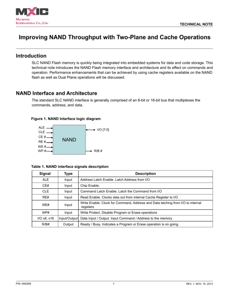
The standard SLC NAND interface is generally comprised of an 8-bit or 16-bit bus that multiplexes the
commands, address, and data.
Figure 1. NAND Interface logic diagram
ALE
CLE
CE #
RE #
WE #
WP #
I/O [7:0]
NAND
R/B #
Table 1. NAND interface signals description
Signal
Type
ALE
Input
Address Latch Enable. Latch Address from I/O
CE#
Input
Chip Enable.
CLE
Input
Command Latch Enable. Latch the Command from I/O
RE#
Input
Read Enable. Clocks data out from internal Cache Register to I/O
WE#
Input
Write Enable. Clock for Command, Address and Data latching from I/O to internal
registers
WP#
Input
Write Protect. Disable Program or Erase operations
I/O x8, x16
R/B#
P/N: AN0268
Description
Input/Output Data Input / Output. Input Command / Address to the memory
Output
Ready / Busy. Indicates a Program or Erase operation is on going.
1
REV. 1, NOV. 15, 2013
TECHNICAL NOTE
Macronix NAND Flash contains an internal Data Register as shown in Figure 2 which is as large as the NAND
page size (2112 Bytes). The Data Register is loaded with data before executing a Program operation or is
used to output the content of the memory after a Read operation is performed. When a Program operation
is started, the Data Register content is programmed inside the Non-Volatile memory NAND array. A Program
operation takes about 250us. When a Read Operation is started, the Data Register is loaded with data from
the Non-Volatile Flash memory. The main array is then programmed with the contents of the data register with
a latency of about 25us.
In addition to the Data Register, a Cache Register is also available in Macronix NAND Products. The Cache
register is the same size as the Data Register and allows for an increased Read and Program throughput by
means of data pipelining. Specific commands enable Cache operations (either Read or Program). The access
to the Cache register can be random and start from any address location. The read or write cycle time to/from
the Data register is as fast as 30ns in Macronix’s SLC NAND MX30LF1G.
Figure 2. NAND Flash Array and Registers
Host
25 ns Data in
Data+Spare
Cache register
Data out 25 ns
Data register
250 us Program
block
Read
25 us
page
Array
Page length can be 512 Bytes often referred to as “Small Page”, 2KB “Large Page” or 4KB page. The most
common SLC NAND is 2KB page. In this document we will refer to “large page” NAND (equal to 2KB) unless
specified.
The Page has extended addressable space often called Spare area used to store ECC parity and other
metadata. For a 2KB page NAND, the spare area is usually 64 bytes. Therefore, each page actually has 2112
Bytes of addressable space.
Currently SLC NAND page size available on the market are:
- 512B page + 16B spare - “small page” - Available only with the smaller densities. Usually the Erase
Block size is 16KB therefore this type of NAND is also referred to as “small block” NAND.
- 2KB page+ 64B spare - “large page” - More commonly available in the market with NAND size from
512Mb to 8Gb. Erase Block size is 128KB.
- 4KB page +224B spare. More commonly available for size greater than 4Gb. Erase Block size is
512KB.
Macronix offers high reliability, high performance “large page” SLC NAND with 2KB page + 64B spare.
P/N: AN0268
2
REV. 1, NOV. 15, 2013
TECHNICAL NOTE
Basic NAND Operations
NAND operations are initiated by first submitting Command cycles to the NAND device. For a complete list of
commands, please refer to Macronix Datasheets on website www.macronix.com.
Typical Commands available in SLC NAND products are listed below. Read and Program Commands will be
explained in more details in the next sections.
Read Commands
- Page Read
- Cache Read Sequential
- Cache Read Random
- Two-plane Read
- Two-plane Cache Read
Program / Erase Commands
- Page Program
- Cache Program
- Two-plane Program
- Two-plane Cache Program
- Block Erase
- Two-plane Block Erase
ID/ Status Commands
- ID Read
- Status Read / Status Enhance Read
- Reset
Other Commands
- Parameter Page Read (ONFI)
- Feature Set Operation (ONFI)
- Unique ID Read (ONFI)
P/N: AN0268
3
REV. 1, NOV. 15, 2013
TECHNICAL NOTE
Command/Address/Data Latching cycles
The standard NAND interface operates on a bidirectional I/O bus. Commands, Address and Data are input or
output on the bidirectional bus. The WE# pin works as a clock signal either in combination with the CLE signal
to latch a command or in combination with ALE signal for address latching (Figure 3).
The minimum Write Cycle time (tWC) is about 25ns (ONFI Mode 4) for SLC NAND such as MX30LF1(2)(4)
G08.
Figure 3. Timing Diagram for Command/Address/Data Latching
CLE, ALE, CE#
tWC
WE#
data/add
data/add
I/O [7:0]
Read Operations
A Read in a SLC NAND is performed on a Page basis. A Read command is used to copy the content of the
flash memory array into the Data Register.
The Read operation is initiated by writing the 00h command and giving the address on I/O[7:0] as shown in
Figure 4. Afterwards, the 30h command is given and the internal read operation begins. The Read Latency
tR (the time needed to transfer the data stored in the non-volatile memory array to the Data Register) for SLC
NAND is about 25us. The data can be read out in sequence after the chip is ready. The data is sent out on
the I/O pins by toggling RE# pin as shown in Figure 4. The minimum Read cycle time tRC is 30ns.
To access the data in the same page randomly, the command of 05h is provided followed by the column
address and confirmation command E0h. After the Data register has been loaded with array content, the Data
Register can be output on the data bus at relatively high frequency by using Data Output commands.
Figure 4. Read Command and Data Output Timing
CLE
WE#
tRC
RE#
I/O [7:0]
00h
A7-A0
A11-A8
A19-A12
A27-A20
30h
Dout n
Dout n+1
tR
busy
R/B#
P/N: AN0268
4
REV. 1, NOV. 15, 2013
TECHNICAL NOTE
Program Operations
The NAND memory is programmed on a Page basis (typically 2K Bytes for Macronix Large Block NAND).
After a Program Load command (80h) is issued and the row and column address is provided, the data will
be loaded into the Data Register sequentially as shown in Figure 5. A Random Write command can also be
issued to load data at a random address in the page. A Program Confirm command (10h) is issued to start the
page program operation. The program latency tPROG is around 250us for SLC NAND products and refers to the
time needed to store the data from the Data Register into the non-volatile array. Because a large amount of
data is programmed during tPROG, the overall throughput of NAND can be very high (ex. 2048B/250us= 8MB/
sec.).
Figure 5.
Data Input and Program Timing
CLE
WE#
RE#
I/O [7:0]
80h
add
add
add
add
add
Din 1
Din n
10h
70h
SR out
tPROG
busy
R/B#
Program Load
Page Program
SR check
In NAND, a Page can be programmed a maximum of NOP (Number of Program) times. NOP indicates the
maximum number of partial program cycles that can occur in a single page, before the page must be erased.
NOP is usually 4 for SLC products and 1 for MLC products. In addition, SLC NAND traditionally requires
1-bit ECC correction over 512 Bytes of data (more precisely, 1-bit correction over 528 Bytes because parity
bits also need to be protected). For these reasons, it is not easy to implement small data chunk logging with
NAND Flash.
Cache Operations
Cache operations are used to enhance Read and Write performance of NAND. Cache Read and Cache
Program commands are available on Macronix NAND families. Cache operations allow us to pipeline Data
Input or Data Output operations, hiding Program or Read latency and enhancing throughput.
In addition to the Data Register, a Cache Register is also available in Macronix NAND Products as shown
in Figure 6. The Cache register has the same size as the Data Register and allows enhancing Read and
Program throughput by means of data pipelining.
Specific commands enable Cache operations (either Read or Program). The access to the Cache register
can be random in some products and start from any address location. The read or write cycle time to/from the
Cache register is as fast as 20ns in Macronix’s SLC NAND MX30LFxG08AB.
P/N: AN0268
5
REV. 1, NOV. 15, 2013
TECHNICAL NOTE
Figure 6. NAND Flash Array and Registers
Host
20 ns Data in
3 us
Data out 20 ns
Data+Spare
Cache register
Cache
transfer
Cache
transfer
Data register
250 us Program
block
3 us
Read
25 us
page
Array
Cache Read
The Cache Read operation is used for read throughput enhancement by means of the internal Cache
Register buffer. Cache Read allows automatic downloading of consecutive pages and reading the entire flash
memory with no additional dead time between pages or blocks. Cache Read can also be performed with
Random addressing in MX30LFxG08AB products. The Read latency is hidden by pipelining data transfers
between Host and Array through the Data and Cache Registers.
After writing the 00h command, the column and row address must be given for the start page selection, and
followed by the 30h command for address confirmation and starting the Cache Read operation. After a latency
time tR, the 31h command is used to move the read page data from Data Register to the Cache Register
with the latency time of tRCBSY (Cache is ready after R/B# High or SR[5]=1, typically after 3us). Then, the
data can be read-out sequentially from 1st column address by toggling RE# pin. The 31h command will also
confirm the next cache read sequential operation (without the need of providing the next page address). After
the data has been output, a new 31h command can be given to read out the next page from Cache Register
and start a new internal Read operation on the subsequent page. The Cache Read Sequential command is
also valid for the consecutive pages across blocks.
Figure 7.
Read Cache Sequential Timing
CLE
WE#
tRC
tRC
RE#
I/O [7:0]
00h
A7-A0
A11-A8
A19-A12
A27-A20
31h
30h
tR
R/B#
P/N: AN0268
Dout 0
tRCBSY
busy
busy
6
Dout 1
Page 0
Dout n
31h
Dout 0
tRCBSY
Dout 1
Dout n
Page 1
busy
REV. 1, NOV. 15, 2013
TECHNICAL NOTE
Figure 8 shows a timing diagram comparison between a Standard Page Read and Cache (page) Read. In a
standard Page Read, the Read latency tR is used here to refer to the internal Read operation (transfer data
from Array to data Register) and must be completed before the data can be output. Using Cache Read to
download the entire page will allow us to completely hide the internal Read transfer from Array to the Data
register. The only latency between the two page data outputs is given by the command latency plus the
latency needed to transfer the Data Register into the Cache Register.
Figure 8. Cache Read vs. Page Read Operation on a 2KB Page NAND
Page Read
Read
Internal operation
Read
Data Output
I/O operation
Data Output
Cache Read
Read
Internal operation
Read
Read
Data Output
I/O operation
Data Output
The improvement obtained in Read throughput using Cache Read compared to normal Page Read is shown
in Figure 9 for a 2KB page and a 4KB page SLC NAND. In this example the throughput improvement is nearly
40% for a 2KB page and 20% for a 4KB page. The reason for the lower improvement for a 4KB NAND is due
to the fact that twice the amount of data must be transferred to the controller while the internal read time stays
the same as for a 2KB page NAND. We can also see that the Cache Read improves the Read throughput on
a 2KB page but is less effective for a 4KB page, under the same conditions.
Figure 9.
Page Read vs. Cache Throughput (tR=25 us, tRC = 25 ns, x8 I/O)
40.0
35.0
2KB page
4KB page
30.0
MB/s
25.0
20.0
15.0
10.0
5.0
0.0
Page Read
P/N: AN0268
Sustained Page Cache Read
7
REV. 1, NOV. 15, 2013
TECHNICAL NOTE
Cache Program
The Cache Program feature enhances the program performance by using the Cache Register buffer. Data
can be input to the Cache Register buffer while the previous data stored in the Data Register buffer is
programmed into the memory. The Cache Program command sequence is almost the same as Page Program
command sequence except the Program Confirm command (10h) is replaced by Cache Program command
(15h).
Once the Cache Program Command is issued, the address and data is loaded into the Cache Register. After
the data input is finished, the Cache Program command (15h) is input, the Cache Register content is moved
into the Data Register and programming of the array starts. The memory Cache Register becomes ready
at this point (the user can check the Cache Status Bit) and new data can be input into the Cache Register
by means of a new Cache Program sequence (command 80h and 15h). When the first page is finally
programmed into the array, the Cache Register is moved into the Data Register, the second page program
starts, and the Cache Register becomes available again for loading the third page to be programmed. If the
user wants to stop, during the Cache Program operation, issue a command 10h instead of 15h.
Figure 10. Cache Program Timing
CLE
WE#
RE#
I/O [7:0]
80h
add
add
add
add
add
Din 1
Din n
15h
70h
SR out
80h
add
add
add
add
add
Din 1
Din n
10h
tPROG
busy
R/B#
70h
SR out
tPROG
busy
Figure 11 shows a timing diagram of the Cache Program operation compared to standard Page Program.
Data input time can be hidden by Program time tP for a 2KB and 4KB page if write cycle time is minimum.
Figure 11. Cache Program vs. Page Program Timing
Page Program
I/O operation
T prog
T prog
Internal operation
Data in
Data in
Cache Program
T prog
Internal operation
Data in
P/N: AN0268
Data in
Cache busy
8
T prog
Data in
Cache busy
Data in
REV. 1, NOV. 15, 2013
TECHNICAL NOTE
Cache Programming can be used to improve the programming throughput with respect to the standard Page
Program. The improvement is about 25% for a 2KB-page SLC NAND but goes up 50% for a 4KB-page
NAND. The improvement in Cache Program is larger for a 4KB page because the amount of data-in is double
with respect to a 2KB-page NAND therefore the pipelining effect is greater. It must be pointed out that the
longer the write cycle time tWC the greater is the advantage of using the Cache Program command as long as
the data-in time is smaller than the programming time TPROG.
Figure 12. Cache Program vs. Page Program (tR=25 us, tWC = 25 ns, x8 I/O)
16.0
14.0
2KB page
4KB page
12.0
MB/s
10.0
8.0
6.0
4.0
2.0
0.0
Page Program
Sustained Cache Program
Dual plane operations
NAND Flash products may support Dual Plane operation. Dual Plane devices can perform Read or Program
operations simultaneously on two pages thus increasing the overall throughput. The memory is divided
into two Planes and each Plane has its own Data and Cache Registers. The two pages that can be read or
programmed simultaneously belong to different Planes. Dual Plane operations use specific commands. The
pages that can be simultaneously Read or Programmed may have addressing restrictions such as when
having the same column address. For details please refer to the datasheet of interest. Macronix 36nm NAND
Flash products support Dual Plane operations.
Dual Plane Read Operation
Dual Plane Read operations are shown in Figure 13 and compared to standard Read and Cache Read
operations. Two pages will be read simultaneously and can be output continuously saving one Read
Operation. Compared to the Cache Read operation, there is little improvement in throughput; a slightly lower
performance can be observed instead because the Read latency cannot be hidden by the data-out. The
maximum throughput is achieved when Dual Plane Cache Read is used and the Read latency is pipelined. In
this case, we see that the Dual Plane Cache Read has the same throughput as Cache Read.
P/N: AN0268
9
REV. 1, NOV. 15, 2013
TECHNICAL NOTE
Figure 13. Dual Plane Read Operation
Page Read
Read
Internal operation
Read
Data Output
I/O operation
Data Output
Cache Read
Read
Internal operation
Read
Read
Data Output
I/O operation
Data Output
Dual Plane Page Read
Read p1/p2
Read p1/p2
Internal operation
Data Output p1
I/O operation
Data Output p2
Dual Plane Cache Read
Internal operation
Read p1/p2
Read p1/p2
Data Output p1
I/O operation
Data Output p2
Data Output p1
The throughput enhancement by Dual Plane operation can be extracted from Figure 13 and is plotted in
Figure 14 for 2KB-page and 4KB-page NAND.
Figure 14. Two Plane Read vs. Single Plane Read (tR=25us, tWC=25ns, x8 I/O)
40.0
2KB page
4KB page
35.0
30.0
MB/s
25.0
20.0
15.0
10.0
5.0
0.0
Page Read
P/N: AN0268
Sustained Page Sustained Dual Sustained Dual
Cache Read Plane Page Read Plane Cache
Read
10
REV. 1, NOV. 15, 2013
TECHNICAL NOTE
Dual Plane Program Operation
Dual Plane Page Program operations can really exploit the benefits of the Dual Plane architecture. A Dual
Plane Program operation is shown in Figure 15. As Programming Time is much longer than the data input
time (e.g. 250us compared to 50us for a 2KB page with tWC of 25ns), the benefit of programming two pages in
parallel is obvious.
For a 2KB page SLC device, the overall programming throughput can be increased by 65% with respect
to the Page Program and 33% with respect to the Cache Program. Dual Plane Cache Program operation
can further boost the throughput of data programming and hide the Data input time inside the programming
phase.
Figure 15. Dual Plane Program Operation
T prog
Internal operation
I/O operation
Data in
plane1
Data in
plane2
Data in
plane1
Data in
plane2
Dual Plane Cache Program
T prog
Internal operation
I/O operation
Data in
plane1
Data in
plane2
Data in
plane1
Data in
plane2
T prog
Data in
plane 1
Data in
Plane 2
Figure 16 compares the different programming methods for 2KB and 4KB devices. We can see that Dual
Plane Program operations can be used to enhance the programming throughput of a 2KB NAND to the level
of a 4KB page NAND.
It is worth noting that the Data-input time is dependent on the write cycle time tWC. If a slower tWC is used (in
this example tWC=25ns), then the Data-in time could become predominant again with respect to the tP time
and the advantage of a Dual Plane Cache Program is diminished.
Figure 16. Two Plane Program vs. Single Plane Program (tR=25us, tWC=25ns, x8)
40.0
35.0
2KB page
4KB page
30.0
MB/s
25.0
20.0
15.0
10.0
5.0
0.0
Page Program
P/N: AN0268
Sustained
Cache Program
Tw o Plane
Program
11
Sustained Tw o
Plane Cache
Program
REV. 1, NOV. 15, 2013
TECHNICAL NOTE
Conclusion
NAND Flash memory is becoming a memory of choice in embedded systems and code storage applications.
This document introduced the NAND Flash memory interface and architecture and described how
taking advantage of NAND Cache registers and Dual Plane operations may significantly improve system
performance.
P/N: AN0268
12
REV. 1, NOV. 15, 2013
TECHNICAL NOTE
Except for customized products which have been expressly identified in the applicable agreement, Macronix's products
are designed, developed, and/or manufactured for ordinary business, industrial, personal, and/or household applications only, and not for use in any applications which may, directly or indirectly, cause death, personal injury, or severe
property damages. In the event Macronix products are used in contradicted to their target usage above, the buyer shall
take any and all actions to ensure said Macronix's product qualified for its actual use in accordance with the applicable
laws and regulations; and Macronix as well as it’s suppliers and/or distributors shall be released from any and all liability arisen therefrom.
Copyright© Macronix International Co., Ltd. 2013. All rights reserved, including the trademarks and tradename thereof,
such as Macronix, MXIC, MXIC Logo, MX Logo, Integrated Solutions Provider, NBit, Nbit, NBiit, Macronix NBit, eLiteFlash, HybridNVM, HybridFlash, XtraROM, Phines, KH Logo, BE-SONOS, KSMC, Kingtech, MXSMIO, Macronix vEE,
Macronix MAP, Rich Au­dio, Rich Book, Rich TV, and FitCAM. The names and brands of third party referred thereto (if
any) are for identification purposes only.
For the contact and order information, please visit Macronix’s Web site at: http://www.macronix.com
MACRONIX INTERNATIONAL CO., LTD. reserves the right to change product and specifications without notice.
P/N: AN0268
13
REV. 1, NOV. 15, 2013
