®
Internal Cache Architecture of
Cache line 0
0
1
X86 Processors
2
Cache line 1
128
or
.
By: K. Goodnow, Ph.D.
Cache line 2
2K - 4K Bytes
256
.
lines
n
DW3
DW2
DW1
16 bytes or 4 doublewords
DW4
Cache Memory
Tag
Memory
Introduction
Figure 2: "Way" Organization
This paper is intended as a reference for the commonalities and differences in internal cache structures in
X86
style
processors.
The
Intel®
486DX
and
IBM
Blue Lightning processors are studied and compared to
highlight the various strategies in cache design.
The
basic structure of these caches and particular instances
are discussed.
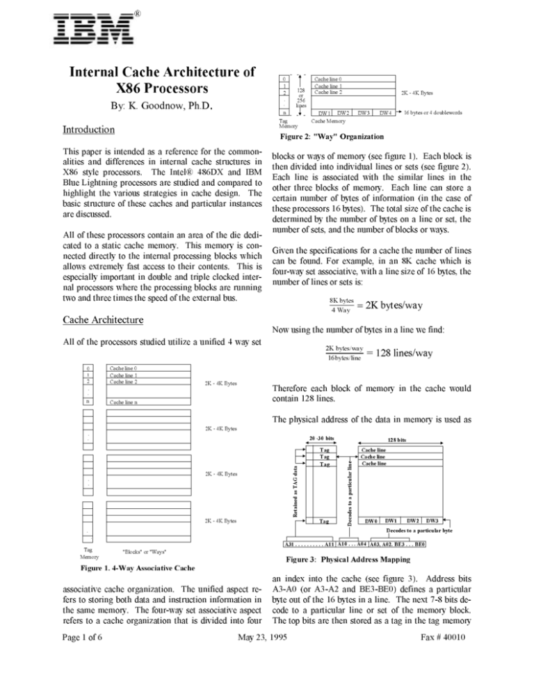
blocks or ways of memory (see figure 1).
Each block is
then divided into individual lines or sets (see figure 2).
Each line is associated with the similar lines in the
other three blocks of memory.
Each line can store a
certain number of bytes of information (in the case of
these processors 16 bytes).
The total size of the cache is
determined by the number of bytes on a line or set, the
All of these processors contain an area of the die dedicated to a static cache memory.
This memory is con-
nected directly to the internal processing blocks which
allows extremely fast access to their contents.
This is
especially important in double and triple clocked internal processors where the processing blocks are running
number of sets, and the number of blocks or ways.
Given the specifications for a cache the number of lines
can be found. For example, in an 8K cache which is
four-way set associative, with a line size of 16 bytes, the
number of lines or sets is:
two and three times the speed of the external bus.
8K bytes
4 Way
= 2K bytes/way
Cache Architecture
Now using the number of bytes in a line we find:
All of the processors studied utilize a unified 4 way set
2K bytes/way
= 128 lines/way
16bytes/line
0
Cache line 0
1
Cache line 1
2
Cache line 2
2K - 4K Bytes
Therefore each block of memory in the cache would
.
.
n
contain 128 lines.
Cache line n
The physical address of the data in memory is used as
2K - 4K Bytes
.
20 -30 bits
.
128 bits
Tag
Cache line
Cache line
Tag
e
ni
Cache line
Tag
taa
l
r
d
la
2K - 4K Bytes
uc
G
.
A
tir
.
T
as
a
p
ed
a
to
ni
se
at
e
d
coe
R
2K - 4K Bytes
Tag
D
DW0
DW1
DW3
DW2
Decodes to a particular byte
.
.
A31 . . . . . . . . . . A11
Tag
A10 . . . A04
A03, A02. BE3 . . . BE0
"Blocks" or "Ways"
Memory
Figure 3: Physical Address Mapping
Figure 1. 4-Way Associative Cache
an index into the cache (see figure 3).
associative cache organization.
The unified aspect re-
Address bits
A3-A0 (or A3-A2 and BE3-BE0) defines a particular
fers to storing both data and instruction information in
byte out of the 16 bytes in a line.
the same memory.
The four-way set associative aspect
code to a particular line or set of the memory block.
refers to a cache organization that is divided into four
The top bits are then stored as a tag in the tag memory
Page 1 of 6
May 23, 1995
The next 7-8 bits de-
Fax # 40010
CATEGORY
BLSX2/SX3
486DX2
IDX2
IDX4
SIZE
16K
8K
8K
16K
PARITY
YES
NO
NO
NO
UNIFIED
UNIFIED
UNIFIED
UNIFIED
4-WAY
4-WAY
4-WAY
4-WAY
SET
SET
SET
SET
ASSOCIATIVE
ASSOCIATIVE
ASSOCIATIVE
ASSOCIATIVE
YES
YES
YES
YES
NO
YES
NO
NO
TYPE
WRITE THROUGH
WRITE BACK
WRITE LEVELS
LINE SIZE
FLUSH TYPES
2
8
4
4
16 BYTES
16 BYTES
16 BYTES
16 BYTES
FULL SNOOP
FULL SNOOP
FULL SNOOP
FULL SNOOP
ADS FLUSH
FLUSH PIN
FLUSH PIN
FLUSH PIN
HOLD FLUSH
SOFTWARE
SOFTWARE
SOFTWARE
SOFTWARE
POWER UP STATUS
OFF
OFF
OFF
OFF
FLUSH ON CLOCK STOP
YES
NO
YES
YES
FULL SNOOP ON CLOCK STOP
YES
NO
YES
YES
NO
YES
YES
YES
CACHE TESTING
Table 1:
for that line.
Cache Architecture Comparison
Each memory block has a 128 or 256 tag
cache, the method of reading and writing to the cache
When checking to see
from the external bus, the invalidation and flushing of
if a particular information byte is stored in the cache,
the cache, and the method of cache coherency during
the line addresses (A11-A4) are decoded to determine
power down mode.
These areas will be covered in the
the tag line memory location to extract the stored ad-
following sections.
Table 1 shows a comparison of the
dress tag and then this tag is compared with the needed
different
physical address upper bits.
processors.
line memory associated with it.
If there is a match, the
cache
architectures
available
in
these
lower address bits are decoded to find the right bytes or
double word.
Cache Size Differences
The 7-8 address bits that are the index to the line or set
The IBM
of a way are repeated every 2048 or 4096 bytes through-
an 8K cache.
out memory.
IBM Blue Lightning 486SX2 and 486SX3 and the Intel
Every repeat of these 7-8 bits can only be
486DX2 and the Intel 486DX2 each contain
This means a line or set size of 128.
stored in that particular line of one of the four "ways."
486DX4 each contain a 16K cache.
This is the main limitation of the four way set associa-
has a line or set size of 256.
tive cache memory architecture.
The
This 16K cache
If the processor asks
for five bytes which are each 2048 or 4096 address
Cache Line Fill
locations away from each other, only four can be held in
cache memory, even if the rest of cache memory is
empty.
When the cache is enabled and the processor requests
data or instruction information that is not present in the
cache, a line fill read is generated.
The line tag and byte addresses are common across all
four of the blocks in the cache, thus the associative nature.
A particular piece of information could be in any
one of the blocks at that particular line.
The tag infor-
mation is the piece that must be checked to ascertain if
If the line is cache-
able the bytes currently requested are fetched from the
system along with the rest of the bytes on that line.
One
of the first places we see a difference in the processors
is in the algorithm used to determine the next set of
bytes to request. The Intel 486DX2 and 486DX4 use an
the data is present and in which particular block.
This cache architecture is common across all of the
processors, the differences are present in the size of the
Page 2 of 6
May 23, 1995
Fax # 40010
Intel specific algorithm that maximizes the double bank
storage for the data."
memory accessing of most motherboards.
will be under operating system control.
These se-
The
quences are shown in table 2.
IBM
Blue
Most of the time this page table
Lightning
486SX2
and
486SX3
also
support the use of a microprocessor specific register
1st
2nd
3rd
4th
(MSR) that controls the cacheability of main memory in
0
4
8
C
64K regions below 1MB and an upper cacheability limit
4
0
C
8
for memory above 1MB.
8
C
0
4
of the caching of memory separate from the other meth-
C
8
4
0
ods.
This
method
is
This allows a coarser control
suitable
for
many
DOS
type
applications.
Table 2: Cache Line Fill Order
Cache Line Replacement
The IBM Blue Lightning 486SX2 and 486SX3 use an
algorithm that maximizes the hit rate for an access to
the next op-code in it's determination of which set of
bytes to request next. These sequences are shown in table 3.
If a cache line fill request is valid, the processor attempts to place the data in one of the four "ways" at that
particular line.
to determine which "way" will be overwritten by the
new
data.
The
LRU
algorithm
uses
several
bits
of
1st
2nd
3rd
4th
0
4
8
C
4
8
C
0
8
C
0
4
will overwrite a line in the cache if it is the least re-
C
0
4
8
cently used among the four "ways."
memory
contained
in
the
tag
line
memory.
The IBM
The processor
486DX2 processor has three external pins,
RPLVAL#,
RPLSET1
and
RPLSET0
which
indicate
the particular "way" that is being invalidated on a new
The cacheability of a particular line of information is
The KEN pin is avail-
able on all of the processors and allows a direct control
of the cacheability of the line.
are
on that line on one of the four "ways."
Cache Line Fill Order
determined by several methods.
that
These bits are changed when there is a memory access
Table 3: IBM Blue Lightning 486SX2 and 486SX3
When set, this pin sig-
nals to the processor that the current address is cacheable.
If all four of the "ways" have that line
occupied a least-recently-used (LRU) algorithm is used
If any byte in a line is un-cacheable, the entire
line is considered un-cacheable.
cache line fill.
If the pin RPLVAL# is set valid it indi-
cates that the values on pins RPLSET1 and RPLSET0
indicate the particular "way" that is being overwritten.
These pins along with the current external address allow an external hardware system to duplicate the internal cache memory data in real time.
Cache Flushing
This "KEN" pin on the Blue Lightning 486SX2 and
486SX3 is shared with a dynamic frequency shifting
function and care must be taken in the system design to
insure that this pin is used as intended for that particu-
cacheability
through software.
ble cache control.
of
a
line
can
also
be
determined
All of the processors support page taThis is a table of the physical ad-
dresses and their mapping.
One bit of this table, the
PCD bit, indicates if this particular page is cacheable.
The PCD bit can be set or reset by the software of the
system.
"Bus Masters" writing to memory is handled by invalidating or flushing the internal cache memory.
This can
be accomplished in two ways, invalidating a particular
lar system.
The
The ability to maintain cache coherency with different
Care must be taken when using the PCD bit
that a cache coherency problem does not arise.
As
line of a single "way" or by invalidating the entire cache
memory.
The first approach of invalidating a single
line is accomplished by checking each valid write address that appears on the bus while another bus master
controls the bus.
Since the entire address needs to be
used, this method is called full snooping.
This method
has the least impact on system performance since only
the particular line of that address cycle is invalidated.
stated in the IBM Blue Lightning manual, "If the PCD
bit
is
changed
dynamically,
the
cache
needs
to
be
flushed to ensure that the processor will go out to main
The second method invalidates the entire cache memory.
This can be accomplished in hardware or software
in all of the processors.
Page 3 of 6
May 23, 1995
The software method relies on
Fax # 40010
the use of the invalidate command in a software program.
The hardware method uses an external signal to
tell the processor to flush the cache.
Write-Through Mode
On the IBM
486DX2, Intel 486DX2 and Intel 486DX4 this external
This method of writing from the processor blocks is the
signal is driven on the FLUSH pin.
least complicated in regards to cache coherency.
The
internal cache and the external system memory are upOn the IBM Blue Lightning 486SX2 and 486SX3 a full
dated at the same time. This method suffers from de-
cache
creased
flush
is
HOLD flush.
accomplished
as
either
an
ADS#
or
The type of flush is set as bits in the
MSR1000 register.
If the full snoop bits are set the
performance
since
an
external
bus
cycle
(usually much slower than the internal cycle time) must
be generated for every write.
If the processor were to
processor will accomplish single line invalidates on a
wait until the external write operation completed before
hold.
continuing, then a write would effectively halt the op-
With the bits set for a HOLD flush, the assertion
of HOLD and HLDA will flush the cache.
With ADS#
eration of the processor.
In order to avoid this bottle-
flush set, the processor will flush on HOLD, HLDA,
neck, write buffers are added to the architecture of the
and ADS# being active.
processor, see figure 4.
This allows a differentiation
between bus master and memory refresh cycles.
cycle.
The CD bit in the control register of the IBM
These write buffers hold the
data, address, and status bits required for the memory
486DX2,
Once the internal processing block passes this
information to the write buffer, it can continue process-
Intel 486DX2, and Intel 486DX4 as well as the CE bit
ing.
in the MSR1000 registers of the IBM Blue Lightning
buffers were full.
486SX2
buffers to the architecture becomes a trade-off between
and
486SX3
enable
and
disable
the
cache.
The only time it would have to wait is if the write
For this reason the addition of write
Disabling the cache causes new non-cached reads to not
performance and silicon area.
enter the cache.
486SX2 and 486SX3 have two write buffers while the
If the cache was previously used and
The IBM Blue Lightning
contains information and if the current address is in the
Intel processors have four write buffers apiece.
cache, the information will be read out of the cache not
IBM 486DX2 contains eight write buffers.
system memory.
The
To disable and not use the cache, the
CE or CD bit must be cleared and then the entire cache
Internally, a write from the processing block is handled
flushed.
as a line modify operation if that physical address is
This flushing can be accomplished through ei-
ther the software or hardware methods discussed.
Write Operations
PROCESSING
BLOCKS
The second type of memory operation is a write into
cache from the processing blocks and a write out to system memory from the processor.
There are two write
modes used in these X86 processors; Write-Through
and Write-Back.
Write-through operation updates the
cache memory (if cacheable) and also writes the data
out to system memory at the same time.
CACHE
A write-back
operation updates the cache (if cacheable) and does not
WRITE
BUFFERS
update the system memory until the modified line is to
be overwritten, the entire cache flushed, or an external
bus master requires access.
This second method means
that writes to a cacheable region stay within the processor.
EXTERNAL
INTERFACE
This reduces the bus activity and subsequently in-
creases the processor performance.
The IBM Blue Lightning 486SX2 and 486SX3, Intel
486DX2, and Intel 486DX4 processors utilize the write-
currently stored in the cache.
through mode.
and is not currently in the cache, the data is written out
ther
The IBM
write-through
or
486DX2 can be set into ei-
write-back
mode.
The
write-
to system memory.
If the data is cacheable
On the Blue Lightning SX2 and
through mode will be discussed first since it is common
SX3 a line fill request for that physical address is then
across all five processors.
made.
Page 4 of 6
May 23, 1995
This approach, known as write-allocate, causes
Fax # 40010
the system memory to be updated first and then that line
asserted.
to be read into the cache.
ing HLDA.
All of the writes will complete before assertThe cache is retained as it was before the
start of the operation.
Although
complicated
internally,
the
write-through
mode does not normally require any system design con-
One problem of using either of the first two methods for
siderations since the effect is that of a non-cached write
cache coherency is if some bus HOLD cycles are not
operation.
memory data cycles.
bus
master
purged
Write-Back Mode
from
µsec).
15
The write-back mode of operation creates a higher performing processor.
access,
the
If refresh cycles are considered a
then
cache
the
at
modified
a
fairly
writes
high
will
rate
be
(every
This may result in little performance gain
over the write-through mode.
Writes to cached memory are at the
speed of the internal processing blocks and are not de-
The
pendent on the external memory cycle time or the num-
physical address on the bus during other bus master cy-
ber of write buffers.
cles.
The IBM
486DX2 is placed in
third
method
of
cache
coherency
checks
each
If a match is found to a cache location that has
this mode by setting the CD bit equal to 0 and the NW
been previously modified the processor will write just
bit to 1 in the CR0 register after reset.
that line back to system memory.
This is accomplished
by issuing cache inquiry cycles to the IBM
486DX2.
The main problem with the write-back mode is cache
The EADS# and INVAL pins are used to issue a cache
coherency.
inquiry
The data in the internal cache could be
more current then the system memory.
If a bus master
to
the
processor.
If
the
cache
contains
the
physical address currently on the bus and some of the
requires that particular information, the data must be
bytes
taken out of the internal cache and written to system
HITM# to signal that the line needs to be written to sys-
memory before allowing the bus master access to that
tem memory.
data.
de-asserted at which time it will write out the modified
If the cache is to be invalidated or flushed, all of
have
been
modified,
the
processor
will
assert
The processor then waits for HOLD to be
the modified data must first be written to system mem-
bytes to system memory.
ory before invalidating the cache.
pact on performance since only those data bytes that are
This method has the least im-
needed are written to system memory.
This method
When the data is modified on a line in cache memory,
does require the ability of the bus master to de-assert
if only some of the data is modified it is marked as par-
HOLD before receiving the information requested and
tially modified.
then re-generate the read request.
This is done on four byte boundaries.
Thus, there are four areas to a line or four double-words
that can be identified as modified.
This means that
Bus Master Write to a Modified Location
when the data needs to be written out to system memory
only those particular double-words that were modified
need be accessed.
If a full-snoop cache invalidation is being used, and a
bus master writes information to a data location that is
Three methods are available in the IBM
486DX2 proc-
essor for cache coherency with the write-back mode.
The first two methods require that all modified memory
locations be written to system memory before releasing
the bus to another bus master.
The first method accom-
plishes this by asserting the FLUSH# pin before asserting HOLD to the processor.
The processor will write
currently cached and has been marked as modified, the
processor can simply mark the line as invalid and accomplish
again.
a
cache
line
fill
if
the
location
is
needed
The modified data would have been over-written
by the bus master in any case.
Power Down Mode Cache Coherency
all previously modified data out of the cache before asserting HLDA.
less
the
The cache will be retained intact, un-
INVAL
pin
is
asserted
when
FLUSH#
is
sampled by the processor in which case the entire cache
is invalidated.
Otherwise the cache continues to be
management
mode.
some
in
extent
order
The
to
processor
save
is
energy.
shut
The
down
to
question
arises, how does the processor maintain cache coherency if a bus master accesses memory during the power
used as if nothing occurred.
The second method uses the BARB bit in the CCR2
register.
All of these processors can utilize some type of power
If this bit is set all modified cache locations
down.
Each of the processors handles this in a different
manner.
are written out to system memory when a HOLD is
Page 5 of 6
May 23, 1995
Fax # 40010
The IBM Blue Lightning 486SX2 and 486SX3 are able
References
to snoop on the bus and flush the cache in both of their
power down modes.
The IBM 486DX2 does not sup-
port snooping or flush during power down mode.
Intel
486DX2
and
486DX4
processors
support
1.
486DX2 Databook, IBM Microelectronics, 1994.
2.
Blue Lightning Microprocessor Data Sheet, IBM
The
both
snooping and flushing during power down.
Microelectronics, 11/1993.
Cache Test Registers
3.
Cache Tutorial, Intel Corporation, 1991.
4.
IntelDX4 Processor Data Book, Intel Corportation,
2/1994.
The internal cache test registers TR3, TR4, and TR5
are present in all of the processors except the IBM Blue
Lightning 486SX2 and 486SX3.
5.
Microprocessors, Vol. 2, Intel Corporation, 1994.
These registers are
used to check the viability of the cache.
Testing of the
cache should be accomplished with the cache turned
off.
Conclusion
This paper has shown the architectural decisions made
on a variety of issues.
The real answer as to the correct-
ness of these decisions is in the performance of the
processor and ultimately the marketplace.
For more in-
formation regarding a particular feature, please consult
the appropriate databook.
IBM Corporation 1995. All rights reserved.
IBM and the IBM logo are registered trademarks of International Business Machines Corporation. IBM Microelectronics is a trademark of the
IBM Corp.
All other product and company names are trademarks/registered trademarks of their respective holders. 1995 IBM Corp.
This document may contain preliminary information and is subject to change by IBM without notice.
for any use of the information contained herein.
tellectual
IBM assumes no responsibility of liability
Nothing in this document shall operate as an express or implied license or indemnity under the in-
property rights of IBM or third parties.
The products described in this document are not intended for use in implantation or other direct life support applications where malfunction
may
result in physical harm or injury to persons.
NO WARRANTIES OF ANY KIND, INCLUDING BUT NOT LIMITED TO, THE IMPLIED WARRANTIES OF
MERCHANTABILITY
OR FITNESS FOR A PARTICULAR PURPOSE ARE OFFERED IN THIS DOCUMENT.
Page 6 of 6
May 23, 1995
Fax # 40010
