APPLICATION NOTE
CHARACTERISTICS OF POWER SEMICONDUCTORS
by J. M. Peter
ABSTRACT
Advantages and disadvantages are summarised,
and the relative cost of each solution indicated.
This paper aims to give a brief overview of the
essential characteristics of power semiconductors,
and to provide a guide in their selection for particular
applications.
Currently, the main types of power semiconductors
are the Power Diode, the power Bipolar Junction
Transistor (BJT), the Thyristor (Triacs and SCRs),
the Gate Turn-off Thyristor (GTO), the Power
MOSFET, and the Insulated Gate Bipolar Transistor
(IGBT).
It considers the characteristics of various power
components when operating like a switch - either
blocking current or voltage, or conducting with a
small voltage drop.
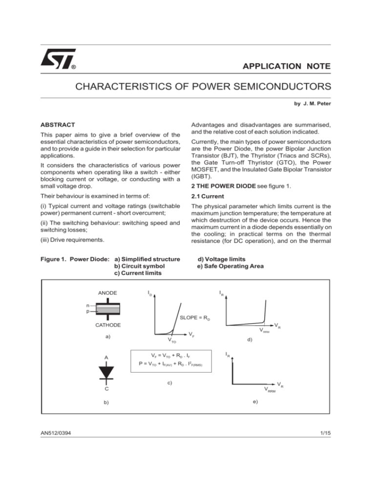
2 THE POWER DIODE see figure 1.
Their behaviour is examined in terms of:
2.1 Current
(i) Typical current and voltage ratings (switchable
power) permanent current - short overcurrent;
The physical parameter which limits current is the
maximum junction temperature; the temperature at
which destruction of the device occurs. Hence the
maximum current in a diode depends essentially on
the cooling; in practical terms on the thermal
resistance (for DC operation), and on the thermal
(ii) The switching behaviour: switching speed and
switching losses;
(iii) Drive requirements.
Figure 1. Power Diode: a) Simplified structure
b) Circuit symbol
c) Current limits
ANODE
d) Voltage limits
e) Safe Operating Area
ID
IR
n
p
SLOPE = R D
CATHODE
a)
A
VTO
V RRM
VF
P = VTO + IF(AV) + RD . I
d)
IR
VF = VTO + RD . IF
2
VR
F(RMS)
c)
VRRM
C
b)
AN512/0394
VR
e)
1/15
APPLICATION NOTE
impedance (for short duration surge currents).
2.2 Voltage
The device is destroyed if the electric field across
the N region of the diode becomes strong enough to
cause breakdown - hence the voltage ratings of the
transistor (forward, VF and reverse, VDRM) depend
upon the thickness of this region.
2.3 Switching
Power PN diodes have a “memory” effect due to the
storage of minority carriers. If the voltage across a
diode which has been conducting in the forward
direction is suddenly reversed, the p and n regions
of the diode are still full of minority carriers, which
can cause the diode to behave like a short circuit for
a short period of time until the minority carrier density
falls. The reverse current due to this effect can
cause problems: current spikes, noise, overvoltages,
and supplementary switching losses.
Figure 2 shows the turn-off behaviour. The main
parameter is the reverse current, IRM, and in some
case the recovery charge Qr. The reverse current
increases with dIR/dt (slope of decreasing current
before turn-off) and with junction temperature.
A fast PN diode is a diode made with a reduced
minority-carrier lifetime, which leads to a reduction
in the diffusion length (ie the average distance
travelled by a minority carrier before recombination).
If the diffusion length is shorter than the thickness of
the silicon N region, the diode’s on-resistance
increases drastically. However the maximum
voltages that the diode can withstand depend upon
the thickness of this region. The design of a fast
diode is therefore the result of a trade-off between
maximum voltage VDRM, forward voltage drop VF and
speed (trr) - see figure 3.
Figure 4 shows losses introduced by a frewheel
diode. Using a faster diode reduces these losses,
but it is not always possible to have an ultra fast
diode with a high voltage rating. Instead it could be
possible to use several low voltage ultra-fast diodes
in series - see reference [3].
When the diode switches off in series with an
inductance L, a supplementary energy L.I2RM is
dissipated in the circuit. For this reason the choice
of circuit configuration is very important (figure 5).
2.4 Schottky Power Diodes
Schottky power diodes, which use only majority
carriers, have a different behaviour; they have a
smaller voltage drop and no recovery charge, and
are many times faster than PN diodes. However,
they have the disadvantages of a limited voltage
range (60 to 100V) and a very high internal
capacitance. The leakage current is also large, and
becomes larger at high temperatures.
Figure 2. Diode turn-off behaviour
IR
Recovery time t
IRM
2/15
rr
Recovery charge Qr
APPLICATION NOTE
Figure 3. Speed versus VDRM
BYW81
BYT12-400
BYT12-800
BYT12-1000
VDRM
200
400
800
1000
VF @ 12V
0.85V
1.4V
1.8V
1.8V
1.8
3.7
6.0
7.8
IRM (A)
Tj = 100oC
dI/dt = -50A/µs
Figure 4. Freewheel diode losses
I trans
+ V
R
-
Vtrans
t d t IRM
I diode
WON(trans) = ½(I + IRM) . (td + tIRM) . VR
VR
I RM
Vdiode
WOFF(diode) =
∫
0
tb
v . i . dt
Figure 5. Effect of circuit topology on diode behaviour
l
+ V
R
-
+ V
R
-
dI F /dt
dI F /dt = VR /2
t IRM
t IRM
I RM
WOFF(diode) =
VR
∫
v . i . dt
VR
WON(trans) = WD + ½ I . I2RM
3/15
APPLICATION NOTE
3 THE BIPOLAR TRANSISTOR see figure 6.
3.2 Voltage
3.1 Current
Two parameters define bipolar transistor voltage
capability:
The current capability is defined by:
VCE(sat) < 1.5V
@
- VCEV, the maximum voltage with the base emitter
junction blocked (VCEV = VCBO, the maximum collectorbase voltage).
IC = IC(sat)
IB= IB(sat)
If IC < IC(sat), the voltage drop VCE is proportional to it,
and can be very small.
- VCEO, the maximum voltage with base open.
If IC > IC(sat), VCE remains relatively constant with
changing IC, and so the transistor can be considered
as a current source.
For switching applications, voltage limits are defined
by the Safe Operating Area (SOA). (VCEW, the working
voltage at high current, is often equal to VCEO).
Maximum capabilities for the early 1990s
The bipolar transistor has no overcurrent capability
(IC cannot exceed IC(max)), and this maximum operating
current is defined by the gain, not by thermal
considerations.
VCEO
VCEV
IC(sat)
Fast transistors
800V
1300V
60A
Slow transistors
1000V
1400V
400A
Figure 6. The Bipolar Transistor: a) Simplified structure
b) Circuit symbol
c) Gain characteristics
C
C
d) Output characteristics
e) Forward breakdown characteristics
f)Forward-bias safe operating area
(FBSOA)
IC
n+
B
n
p
n+
E
E
B
a)
GAIN
VCBO
VCEO
b)
VCE
c)
IC
IC
VBE
I C(SAT)
d)
4/15
V CE
VCE
VCE(SAT)
e)
f)
APPLICATION NOTE
Voltage drop: If IC < IC(sat) the voltage drop (with
optimised drive) is very low.
VCE =
____IC____
IC(sat) . VCE(sat)
in the data sheets.
The following empirical relation can be used to
estimate gain at other current levels.
ß @ IC = [ß @ IC(sat)] .
3.3 Drive requirements
_IC_
IC(sat)
See figure 7.
3.4 Switching times
The BJT is a current-driven device: during the
conducting phase its necessary to deliver a base
current
The total turn-off time toff is the sum of two
components (see figure 8):
IB1 = _IC_
ß
ß = gain
At nominal current the gain specified for low voltage
transistors (VCEO < 250V) is around 10, and for high
voltage transistors is around 5, near IC(sat) as defined
- The storage time ts. This is a “memory” effect, due
to the storage of minority carriers in the base. (1s for
VCEO = 100V, 3s for VCEO = 400V).
- The fall time tf. The majority of switching losses are
due to the fall time (but modern transistors using
cellular technology have very small fall times).
Figure 7. Driving a bipolar transistor: a) Driving circuit
b) Choosing the base drive current
TURN ON
GAIN
IB
I C(sat)
I B(sat)
TURN OFF
I C(sat)
3V
IC
b)
a)
Figure 8. Bipolar transistor switching times
IB
To ensure fast turn-off, it is necessary to force a
negative current IB2 in the base to increase the rate
of recombination of minority carriers.
3.5 The Darlington
ts
This is a structure which behaves like two bipolar
transistors connected, as shown in figure 9: the first
acting as a driver, and the second as a power stage.
IC
tf
The Darlington offers higher gain than a conventional
BJT, and the ability to operate at higher current
density (because the gain of the power stage can be
very high), but these advantages are offset by a
5/15
APPLICATION NOTE
Figure 9. Darlington Transistor characteristics
a) Equivalent structure
b) Output characteristics
c) Gain characteristics
Standard
BJT Darlington
V CE
2.5V
behaves like two bipolar transistors connected back
to back, which once fired effectively provide their
own base drive current.
4.1 Current
The maximum operating current is defined, like the
power diode, by the rate at which the device is
cooled. The thyristor can withstand very high surge
currents (within the capabilities of the cooling
arrangements).
4.2 Voltage
a)
I C(sat)
IC
b)
The blocking voltage can be very high - up to 5kV.
Its voltage drop is around 0.8V at low current, rising
to 1.2V at nominal current.
4.3 Drive requirements - see figure 11.
Gain
IC
c)
Because of the positive feedback, the thyristor needs
only a very low current for a short time at turn-on
(firing). In practice a small “holding current” is required
to maintain the device in conduction. However it has
the disadvantage that the device cannot be turned
off by controlling the gate current - instead the anode
current must be forced to zero, by forcing the anodecathode voltage to zero. In switching or AC circuits
this can be achieved using a resonant LC circuit
connected in series or parallel.
4.4 Switching times
higher voltage drop:
VCE(sat) Darlington = 0.8V + VCE(sat) BJT
and also the increased turn-off time - the power
stage transistor can only begin to turn off after the
driver has turned off.
4. THE THYRISTOR
“Thyristor” is a generic term for a semiconductor
device having four or more layers. The two main
members of the family are the Silicon Controlled
Rectifier, or SCR (often simply called a thyristor)
and the TRIAC (derived from TRIode for Alternating
Current). Both share similar current and voltage
characteristics. The structure and characteristics of
the SCR are shown in figure 10.
The thyristor operates using positive feedback once the device is turned on or “fired” by applying
the current pulse to the gate, it continues to conduct
until the current through it falls below a certain small
fixed value, known as the holding current. This effect
occurs because, as shown in figure 10b, the SCR
6/15
When the anode current is forced to zero, the thyristor
turns off. However, it is necessary to wait for a time
tq (the turn-off time, like the fall time of a bipolar
device) before the anode voltage is reapplied otherwise the device will continue to conduct.
4.5 The TRIAC
The TRIAC is effectively two SCRs connected in
anti-parallel, with a single gate - see figure 12. This
device can conduct current in both directions (ie
from A1 to A2 and from A2 to A1) and so can be
used to control the flow of AC currents - the current
through the device will fall below the holding current
every half cycle, and at this point the device will turn
off automatically unless it is refired. Hence for
continuous conduction the device must be refired at
twice the frequency of the current it is conducting.
As shown in figure 13, the TRIAC can operate in one
of two ways:
a) The device is fired on only for a certain proportion
of AC half waves, or
b) The firing of the device can be delayed such that
APPLICATION NOTE
Figure 10. The SCR:
a) Simplified structure
b) Equivalent circuit
c) Circuit symbol
d) Current limits
e) Voltage limits
f) Switching Safe Operating Area
A
A
p
n
T2
p
n+
T1
G
C
G
C
a)
b)
c)
IA
IA
VT
VAWM
ρ
e0
VDWM
IA
VDWM
V AWM
d)
e)
f)
Figure 11. Thyristor drive requirements
A
IG
G
3V
C
IA
7/15
APPLICATION NOTE
Figure 12. The TRIAC a) Simplified structure
b) Circuit symbol
c) Equivalent circuit
A1
Gate
n
p
A1
A1
n
Gate
n
n
p
Gate
Gate
A2
A2
A2
a)
Figure 13. Driving a TRIAC:
b)
c)
a) Using as an on-off switch
b) Phase control
Original AC
signal
TRIAC drive
signal
Resulting
output
a)
only a portion of each half wave is allowed through.
This is known as phase control.
Operating in the first way, the device can be used
as a simple on-off AC switch, while used in the
second way, the device can be used to control AC
power - for example as a speed control for an AC
motor.
5 THE GTO see figure14.
The GTO is another “positive feedback” component
and is similar to the thyristor, but it has an
8/15
b)
interdigitated structure, as shown in figure 14.
Consequently it has similar characteristics to the
thyristor, but it can be blocked like a transistor.
5.1 Voltage
GTOs can support up to around 4kV with a maximum
rated current of 1kA. During turn-off the maximum
voltage is defined by the SOA. The GTO has a poor
S.O.A. when operating at high currents. Its voltage
drop is marginally higher than that of the thyristor.
5.2 Drive requirements see figure 15.
APPLICATION NOTE
Figure 14. The Gate Turn-Off Thyristor:
a) Simplified structure
b) Equivalent circuit
c) Circuit symbol
d) Current limits
e) Voltage limits
A
A
A
p
n
p
n+
G
G
G
C
C
C
a)
b)
VT
c)
IA
ρ
e0
V AWM
IA
V DWM
d)
e)
Figure 15. Driving a GTO
Figure 16. GTO switching times
A
IG
G
IG
6V
l
20V
C
ts
IA
tail effect
Figure 15
Figure 16
9/15
APPLICATION NOTE
constant of cooling arrangements (figure 18).
The GTO requires a very high negative gate current
to turn-off quickly; its has a gain of only 3 which
means it requires a sophisticated and expensive
gate drive if it is to be run at any speed. This means
that it is often impractical to use a charge extracting
drive circuit, and so the device has a “tail effect”
whereby the device still conducts while the minority
carriers combine naturally.
6.2 Voltage
Because the area of silicon used and hence RDS(ON)
increase considerably with the maximum rated
voltage, this voltage is currently limited to around
1000V.
5.3 Switching times see figure 16
The MOSFET has a large S.O.A, as it is able to
sustain its maximum rated voltage during turn-off.
Like the bipolar transistor the GTO has a storage
time, and during the fall time its tail effect considerably
increases the turn-off losses.
Present technology current ratings are governed by
the following RDS(ON) (25oC) values for the relevant
voltage ranges.
6 THE POWER MOSFET see figure 17.
RDS(ON) @ 25oC
This component uses only majority carriers in
conduction, which accounts for its specific behaviour.
The majority carriers flow into the component due to
the influence of gate voltage; the current cannot be
limited by a “gain phenomenon”. Hence the voltage
drop depends only on the resistance of the silicon
path between the drain and source, RDS(ON).
Max. rated voltage
(mW)
(V)
77
100
850
500
3500
1000
6.1 Current
The maximum operating current is defined, as for a
diode, by the rate at which it is cooled. Its surge
current capabilities are defined by the thermal time
Figure 17. The Power MOSFET:
a) Simplified structure
b) Circuit symbol
c) Equivalent circuit
d) Output characteristics
e) Forward breakdown characteristics
f) Switching Safe Operating Area
D
D
n+
np+
≈
G
n+
G
S
S
G
a)
ID
b)
ID
ID
R ON
V DS
d)
10/15
c)
V DSS
e)
V DS
VDSS
f)
V
APPLICATION NOTE
Figure 18.Turnoff with high current
6.3 Drive requirements
During conduction the gate requires only a voltage
(approximately 15V) without any significant
energy consumption - see figure 19.
MOSFETs turn off very quickly when the gate-source
voltage falls to zero. However, the prescence of a
capacitance between the gate and source means
that to switch the device, charge must be supplied or
removed to make the gate voltage rise or fall.
I DS ,10A/Div
VDS , 200V/Div
The designer must consider losses due to the charge/
discharge of this capacitance at each turn-on/off.
50ns/Div
6.4 Switching times
It is frequently said that the MOSFET has a very
high voltage drop, but this is not correct. The
MOSFET voltage drop, RDS(ON).I, can be very low at
a low current density, though that would be
compensated by the need for a large silicon surface
area.
The R DS(ON) is (unfortunately) specified in
manufacturers datasheets at 25oC. At a more realistic
operating temperature:
Figure 19: a) Driving a Power MOSFET
G
S
The IGBT can be considered as a pseudo-Darlington
with a MOSFET as driver and a bipolar transistor as
the power stage.
7.1 Current
b) MOSFET switching waveforms
V GS
+
-
7 THE IGBT see figure 20.
The maximum current is generally limited by cooling.
It has over-current capability.
RDS(ON) @ 100oC ≈ 1.7 x RDS(ON) @ 25oC
D
The MOSFET, a majority carrier device, has no
storage time. This is very important for many
applications. Fall time (depending on drive) can be
very small, but for a rated voltage higher than 300V,
it is approximately the same for both fast bipolar and
MOSFET devices.
IG
Effect of gate-source capacitance
Gate voltage +15V
(Logic level MOSFET +5V)
ID
No storage time
a)
b)
11/15
APPLICATION NOTE
Figure 20. The IGBT: a) Simplified structure
b) Circuit symbol
c) Equivalent circuit
d) Output characteristics
e) Forward breakdown characteristics
f) Switching Safe Operating Area
D
C
p+
C
n+
np+
G
G
n+
E
E
G
G
S
a)
b)
c)
ID
VDS
ID
3ID
ρ
ID
VDSS
ID
d)
7.2 Voltage
At present, the maximum rated voltage is 1.2kV.
This limit is rapidly increasing towards 1800V and a
maximum rated current of 500A. The SOA is
approximately rectangular.
The voltage drop across the IGBT is relatively
constant with respect to the current. This means
that at high current levels, conduction losses are
lower than those of a MOSFET, but at low current
levels they are considerably higher. This causes a
limit to the efficiency of IGBT circuits.
V DS
VDSS
e)
V
f)
Figure 21. Driving an IGBT.
a) Driving circuit
b) Switching waveforms
VGS
15V +
-
IG
Tail
ID
7.3 Drive requirements
Similar to the MOSFET drive (figure 21).
a)
b)
7.4 Switching times
The MOSFET stage has practically no storage time,
but the bipolar section causes a tail current like that
in the GTO, where the device continues to conduct
due to the prescence of residual minority carriers in
the base. As the base section of the device cannot
12/15
be accessed externally to remove these charges,
this tail current persists until the carriers recombine
naturally. This current causes switching losses,
which increase with operating frequency.
APPLICATION NOTE
Figure 22. IGBT Switch-off behaviour:
a) Normal current
b) Very high surge current
IC
IC
V CE
V CE
ID
= 2A / Div
VDS = 100V / Div
t
= 200ns / Div
ID
= 10A / Div
VDS = 100V / Div
t
= 500ns / Div
a)
b)
8. LIMITS AND MAXIMUM RATINGS
take into account a number of factors, such as:
The absolute maximum ratings are defined by the
semi conductor manufacturer. These ratings must
not be exceeded under any circumstances - to do so
risks destroying the component. Examples of
maximum ratings are the maximum junction
temperature Tj(max), the maximum current and the
maximum blocking voltage.
i) The cost of the device, and the cost constraints on
the application.
It should be noted that the user cannot measure
these parameters, as the device will probably be
destroyed in the attempt. Characteristics which may
be measured are for example the collector-emitter
saturation voltage VCE(sat), and the switching times.
The manufacturer specifies a maximum and/or
minimum value, depending on the parameter. In the
design of circuits it is important to take into account
the “worst case” value of the component, and to
verify that the circuit operates correctly with the
spread of all parameters.
9. CHOOSING THE RIGHT SEMICONDUCTOR
When selecting the type of semiconductor device to
use in a particular application, the designer must
ii) The magnitude of voltages and currents
encountered.
iii) The drive requirements of the device - the need
for a complex drive circuit can increase design time
and the cost of the circuit.
iv) The frequency at which the device will switch.
9.1 Typical applications of each type
9.1.1 Bipolar transistors
In general terms bipolar transistors compete with
Power MOSFETs and IGBTs. Their main advantage
over these types is the lower cost, particularly for
high voltage devices, while their main disadvantages
are the cost of the drive circuit and the limit on their
switching speed imposed by the storage and fall
times. The applications in which they are used are
typically characterised by low to medium operating
frequency and high voltage, where they result in a
cheaper solution than the equivalent MOSFET or
13/15
APPLICATION NOTE
IGBT. Examples are in electronic lamp ballasts,
automotive ignition switches, and horizontal
deflection circuits in TVs and monitors.
9.1.2 Power MOSFETs
The main advantages of Power MOSFETs are their
minimal drive requirements and ability to operate at
high frequencies. In power supplies, operation at
high frequencies allows the size of circuit magnetics
to be reduced, decreasing the circuit cost. In compact
fluorescent lamp ballasts (such as those used in
domestic environments) operating at high
frequencies leads to smaller overall dimensions.
The low currents and relatively low voltages in this
application means that in this case the Power
MOSFET leads to a cheaper solution than the power
bipolar.
Power MOSFETs are also frequently used as power
actuators (solid-state relays) in automotive circuits,
because of the low voltages involved means that
they are inexpensive, and types are available which
can be driven directly from a microprocessor, which
are increasingly being used to control automotive
systems.
9.1.3 IGBTs
The main applications of IGBTs are in motor control
and automotive ignition - again these are
characterised by high voltages and relatively low
operating frequencies. In these applications they
compete with bipolars. Although the basic device is
more expensive than a bipolar transistor, the minimal
drive requirements can lead to a cheaper overall
solution, particularly where there is a need to interface
with a microprocessor. Its main disadvantage is the
unavoidable losses caused by the tail current (which
become more significant at high frequencies),
9.1.4 GTOs
GTOs are used in conditions of very high voltage
and very high current, and low switching frequencies.
An example of their use is in electric trains.
9.1.5 Thyristors
This component is very cheap, but its use is limited
by the difficulty of turning it off. It can be used to
control devices which can be fed with half-wave
rectified AC current, for example DC motors (when it
will turn off automatically every half cycle, like the
TRIAC), and also to protect other devices, for
example in power supplies.
14/15
9.1.6 TRIACs
TRIACs are unique in their ability to conduct and
control current in both directions. They are the
cheapest way of controlling AC currents, for example
in AC motor speed controls or lamp dimmers.
11. CONCLUSION
“Power MOSFET has very high voltage drop”
“Bipolar ... an old technology”
“Epitaxial is better...”
This type of commercial jargon does not help the
designer to produce optimal circuits. At the present
time the designer has a choice between a lot of
components. Which is the best solution? The answer
is, there is no best solution - this is the field of
technical design, not scientific research.
For some applications, for example 1MHz Switch
Mode Power Supplies, only one solution (MOSFET)
is possible. For most applications, there are always
several solutions. The designer’s job is to optimize
the “switching function”after thorough analysis.
Experience shows that the quality of this analysis,
and the work done by the designer (drive, protection,
etc.) play a bigger role in the total cost than the
actual price of the component.
REFERENCES
[1] Transistors and Diodes in Power Processing
THOMSON SEMICONDUCTOR 1985
[2] Power Transistor application manual
SGS-THOMSON 1989
[3] Parallel Operation of Fast Rectifiers
SGS-THOMSON Application Note
APPLICATION NOTE
Information furnished is believed to be accurate and reliable. However, STMicroelectronics assumes no responsibility for the consequences
of use of such information nor for any infringement of patents or other rights of third parties which may result from its use. No license is
granted by implication or otherwise under any patent or patent rights of STMicroelectronics. Specification mentioned in this publication are
subject to change without notice. This publication supersedes and replaces all information previously supplied. STMicroelectronics products
are not authorized for use as critical components in life support devices or systems without express written approval of STMicroelectronics.
The ST logo is a trademark of STMicroelectronics
1999 STMicroelectronics - Printed in Italy - All Rights Reserved
STMicroelectronics GROUP OF COMPANIES
Australia - Brazil - China - Finland - France - Germany - Hong Kong - India - Italy - Japan - Malaysia - Malta - Morocco Singapore - Spain - Sweden - Switzerland - United Kingdom - U.S.A.
http://www.st.com
15/15
