P9813 Datasheet
advertisement
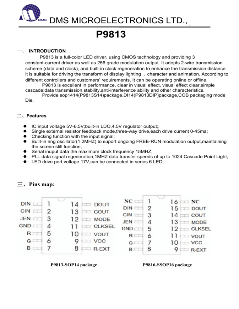
DMS MICROELECTRONICS LTD., P9813 一、 INTRODUCTION P9813 is a full-color LED driver, using CMOS technology and providing 3 constant-current driver as well as 256 grade modulation output. It adopts 2-wire transmission scheme (data and clock), and built-in clock regeneration to enhance the transmission distance. it is suitable for driving the transform of display lighting 、character and animation. According to different controllers and customers’ requirements, It can be operating online or offline. P9813 is excellent in performance, clear in visual effect, visual effect clear,simple cascade;data transmission stability,anti-interference ability and other characteristics. Provide sop1414(P9813S14)package,DI14(P9813DIP)package,COB packaging mode Die. 二、Features z z z z z z z IC input voltage 5V-6.5V;built-in LDO,4.5V regulator output;; Single external resistor feedback mode,three-way drive,each drive current 0-45ma; Checking function with the input signal; Built-in ring oscillator(1.2MHZ) to suport ongoing FREE-RUN modulation output,maintaining the screen still function; Serial inuput data the maximum clock frequency 15MHZ; PLL data signal regeneration,1MHZ data transfer speeds of up to 1024 Cascade Point Light; LED drive port voltage 17V,can be connected in series 6 LED; 三、Pins map: P9813-SOP14 package P9816-SSOP16 package DMS MICROELECTRONICS LTD., 四、Pin function description(P9813 S14\DIP14) Pin Symbol Function 1 2 Din Cin Serial data input. Built-in pull. high 3 JEN 4 GND 5,6,7 R,G,B 8 R-EXT Adjustable output current resistance 9 VCC Supply voltage,5-6.5V 10 VOUT Internal operating voltage.VCC>5V time,5V regulator output,while VCC<5V 11 CLKSEL CLKSEL=1,output clock back,CLKSEL=0,output clck forward 12 MODE 13 14 COUT DOUT Serial clock input, built-in pull. high JEN=1,timing no parity,JEN=0,timing verification,drive mode,built-in pull-up GDN RGB output of three=way drive external feedback mode,access resistance MODE=1,output is constant current drive mode,mode=0,output is the plug-in constant pressure Serial clock output. Serial Date output. 五、P9813 communication protocol 32bit gray data for the first pixel 32bit gray data for the 2nd pixel DMS MICROELECTRONICS LTD., 1. The ic will latch a bit of data when the rising edge of the clock coming, And the data should changed after the falling edge of the clock; 2. The flag bits is two “1”; 3. The verify dta B7’is equal to ~B7,and B6’1S ~B6,B7 and B6 are the gray data of blue 4. the serial data is MSB first ,and the sortorder is blue ,green, red 六、ELECTRICAL PARAMETERS DMS MICROELECTRONICS LTD., 七、Resistor to adjust the input current As shown,IC connected through a resistor to adjust the external input current I Current adjust the resistor DMS MICROELECTRONICS LTD., Typical resistor values: Resistance Output Current 24KΩ 10KΩ 6.8KΩ 20mA 36mA 46mA 八、Typical Applications; 1.simple circuit (small point source) The circuit drive current from the RF resistance adjustment 0-45mA,and CLKSE,MODE ports are vacant ,JEN port parity enable,choose according to customer needs PS:RD,RC,RV resistance were selected to 39Ω,39Ω,3.6Ω DMS MICROELECTRONICS LTD., 2. P9813 12V applications: Dotted line part can be omitted,which according to the customer to modify the actual situation.output current adjustment method according to the “seven,resistance to adjust output current” 3 .P9813 24V applications: Dotted line part can be omitted,which according to the customer to modfiy the actual situation.Output current adjustment method according to the“seven,resistance to adjust output current” DMS MICROELECTRONICS LTD., 5. Plug-in constant voltage drive mode/among all the way to the output as an example) This mode is the case for multi-led,in fact,through the R-side output level control external NPN transistor to drive multiple LED Limiting resistor calculation-R=(VDD-VLED-VCE)/18mA Work in the switch area where the transistor,VCE is the transistor saturation voltage,and generally 0.5V-0.8V.the base resistance RB desirable 2K-5K,in front of other signal connections to the same pattern.VLED single lamp is generally preferable to red light:1.8V-2V,green;3V-3.5V,blue light:3V-3.5V The model commonly used in multi-channel”first string and the” connection,in view of any one LED in series branch circuit,it will lead to slip all the LED is off ,so the use of the connection should follow the following principles;slip LED series number is generally 3 to6,should be more not less parallel branches. Jen enable clients to choose according to customer neeeds. 6. Cascade signal driver capability,and connection method ■ As chip desingn push-pullo drive circuit ,making the cascade signal drive capability have increased significantly.Twisted pair is recommended to increase the transmission distance.To enhance the anti-interference ability in the position near the IC input, the addition of two 20P decoupling capacitors. ■ Proposed transmission close at DOUT and COUT mouth and then output to the lower series resistance in order to prevent signal reflection;operating voltage in the 4.5V-12V with resistance to 39Ω resistor,the resistance should be installed close to the IC’s output DMS MICROELECTRONICS LTD., ■ Application of small point source (F8 poit source),the propose power between the chip VCC pin plus a 3.6Ω resistor (RV),Add a resistor ,VDDin the 5V-5.3V,it can effectively reduce human error led to the VDD and GND short-circuit burned IC ■ Recommended operating voltage 24V,DIN and CIN in the mouth of the ESD protection tube connected to protect against high input voltage damage. 九:Package size P9813 (SOP-14) DMS MICROELECTRONICS LTD., P9813 (DIP -14)

