Symbols and Terms
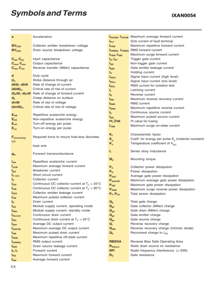
a
Acceleration
BVCES
BVDSS
Collector emitter breakdown voltage
Drain source breakdown voltage
Cies, Ciss
Coes, Coss
Cres, Crss
Input capacitance
Output capacitance
Reverse transfer (Miller) capacitance
d
dA
di/dt, -di/dt
(di/dt)cr
diF/dt, -diF/dt
dS
dv/dt
(dv/dt)cr
Duty cycle
Strike distance through air
Rate of change of current
Critical rate of rise of current
Rate of change of forward current
Creep distance on surface
Rate of rise of voltage
Critical rate of rise of voltage
E AR
EAS
E off
Eon
Repetitive avalanche energy
Non-repetitive avalanche energy
Turn-off energy per pulse
Turn-on energy per pulse
F(mounting)
on
Required force to mount hole-less discretes
heat sink
gfs
Forward transconductance
IAR
IAVM
IBO
IC (on)
IC
IC25
IC90
ICES
ICM
ID
IDD
IDD0
ID(cont)
ID25
IDAV
ID(AV)M
IDM
IDRM
ID(RMS)
IDSS
IF, IT
IFM
IFAV
Repetitive avalanche current
Maximum average forward current
Breakover current
Short circuit current
Collector current
Continuous DC collector current at TC = 25°C
Continuous DC collector current at TC = 90°C
Collector emitter leakage current
Maximum pulsed collector current
Drain current
Module supply current, operating mode
Module supply current, standby mode
Continuous drain current
Continuous drain current at TC = 25°C
Average DC output current
Maximum average DC output current
Maximum pulsed drain current
Maximum repetitive off-state current
RMS output current
Drain source leakage current
Forward current
Maximum forward current
Average forward current
XX
IXAN0054
IF(AV)M, IT(AV)M
IFLT
IFRM
IF(RMS), IT(RMS)
IFSM, ITSM
IG, IGT
IGD
IGES
IH
IIN(H)
IIN(L)
IISOL
IL
IR
IRM
IRMS
IRRM
IS
ISM
I²t, ∫i²dt
ITSM
Maximum average forward current
Sink current of fault terminal
Maximum repetitive forward current
RMS forward current
Maximum surge forward current
Trigger gate current
Non-trigger gate current
Gate emitter leakage current
Holding current
Signal input current (high level)
Signal input current (low level)
RMS current for isolation test
Latching current
Reverse current
Maximum reverse recovery current
RMS current
Maximum repetitive reverse current
Continuous source current
Maximum pulsed source current
I²t value for fusing
Maximum surge on-state current
Kf
Kp
KT
Characteristic factor
Coeff. for energy per pulse Ep (material constant)
Temperature coefficient of VBO
L
Series stray inductance
Md
Mounting torque
PC
PD
PGAV
PG(AV)M
PGM
PRSM
PT, Ptot
Collector power dissipation
Power dissipation
Average gate power dissipation
Maximum average gate power dissipation
Maximum gate power dissipation
Maximum surge reverse power dissipation
Total power dissipation
Qg
Qgc
Qgd
Qge
Qgs
Qr
QRM
QS
Total gate charge
Gate collector (Miller) charge
Gate drain (Miller) charge
Gate emitter charge
Gate source charge
Reverse recovery charge
Reverse recovery charge (intrinsic diode)
Recovered charge to IRM
RBSOA
R DS(on)
RFI
RG
Reverse Bias Safe Operating Area
Static drain source on resistance
Radio frequency interference (= EMI)
Gate resistance
Symbols and Terms
RGE
rT
RthCK; RthCH
R thJA
RthJC
RthJK; RthJH
RthJS
R thJW
R thKA
Gate emitter resistance
Slope resistance (for power loss calculation
only)
Thermal resistance case to heatsink
Thermal resistance junction to ambient
Thermal resistance junction to case
Thermal resistance junction to heatsink
Thermal resistance junction to heatsink
Thermal resistance junction to water
Thermal resistance heatsink to ambient
SCSOA
Short Circuit Safe Operating Area
Tamb, TA
TC, Tcase
t d(off)
t d(on)
tfi
tfr
tFLT
tgd
TJ, TVJ
TJM, TVJM
TK,TH, TS
TL
TS(max)
Tstg
tP
tq
tr
trr
trv
tSC
Ambient (cooling medium) temperature
Case temperature
Turn-off delay time
Turn-on delay time
Current fall time (inductive load)
Forward recovery time
Overcurrent or short circuit trip delay time
Gate controlled delay time
Virtual junction temperature
Maximum virtual junction temperature
Heatsink temperature
Lead temperature
Maximum allowable heatsink temperature
Storage temperature
Pulse time
Turn-off time
Current rise time
Reverse recovery time
Rise time of collector emitter voltage
Short circuit duration
VBO
VCE
VCE(sat)
VCE(sat)FLT
Breakover voltage
Collector emitter voltage
Collector emitter saturation voltage
Collector emitter saturation voltage to indicate
fault
Collector emitter clamp voltage on chip level
Collector emitter voltage
Collector gate voltage
Module supply voltage
Module supply voltage without fault
Drain gate voltage
Maximum repetitive forward blocking voltage
Drain source voltage
Maximum non-repetitive forward blocking
voltage
Drain source breakdown voltage
Various construction designs of products
VCEK
VCES
VCGR
V DD
VDD FLT
VDGR
V DRM
VDS
VDSM
VDSS
Version
IXAN0054
VF
VFLT
VFR
VGD
VGE
VGE(th)
VGEM
VGES
VGS
VGS(th)
VGSM
VGT
VH
VIN
VIN(H)
VIN(L)
VISOL
VR
VRES
VRGM
V RRM
VRSM
VSD
VT
VT0
Forward voltage
Voltage at fault terminal
Forward recovery voltage
Gate non-trigger voltage
Gate emitter voltage
Gate emitter threshold voltage
Maximum transient collector gate voltage
Maximum DC gate voltage
Gate source voltage
Gate threshold voltage
Maximum transient gate source voltage
Gate trigger voltage
Holding voltage
Input control voltage
Input voltage threshold for IGBT turn-on
Input voltage threshold for IGBT turn-off
Isolation voltage
Reverse voltage
Input voltage threshold for Reset = active
Maximum reverse gate voltage
Maximum repetitive reverse voltage
Maximum non-repetitive reverse voltage
Forward voltage drop
Forward voltage
Threshold voltage (for power loss calculation)
ZthJC
ZthJK, ZthJH
Transient thermal impedance junction to case
Transient thermal impedance junction to
heatsink
Semiconductor Catalog, Edition 2006
© IXYS Corporation 2006
All Rights reserved
Note
As far as patents or other rights of third parties are concerned,
liability is only assumed for components per se, not for applications,
processes and circuits implemented with components or assemblies.
The information describes the type of component and shall not be
considered as assured characteristics.
Stress above one or more of the limiting values may cause permanent damage to the device. These are stress ratings only and
operation of the device at these or at any other conditions above
those given in the characteristics sections of the specification is not
implied. Exposure to limiting values for extended periods may affect
device reliability. Terms of delivery and rights to change design or
specifications are reserved.
Changes have been made to earlier published specifications. The
data herein supersedes all previously published informations.
Life support applications
IXYS products used in life support appliances, devices, or systems
where malfunction of these products can reasonably be expected to
result in personal injury must be expressly authorized for such
purposes.
XXI
