ZXCT1010
advertisement
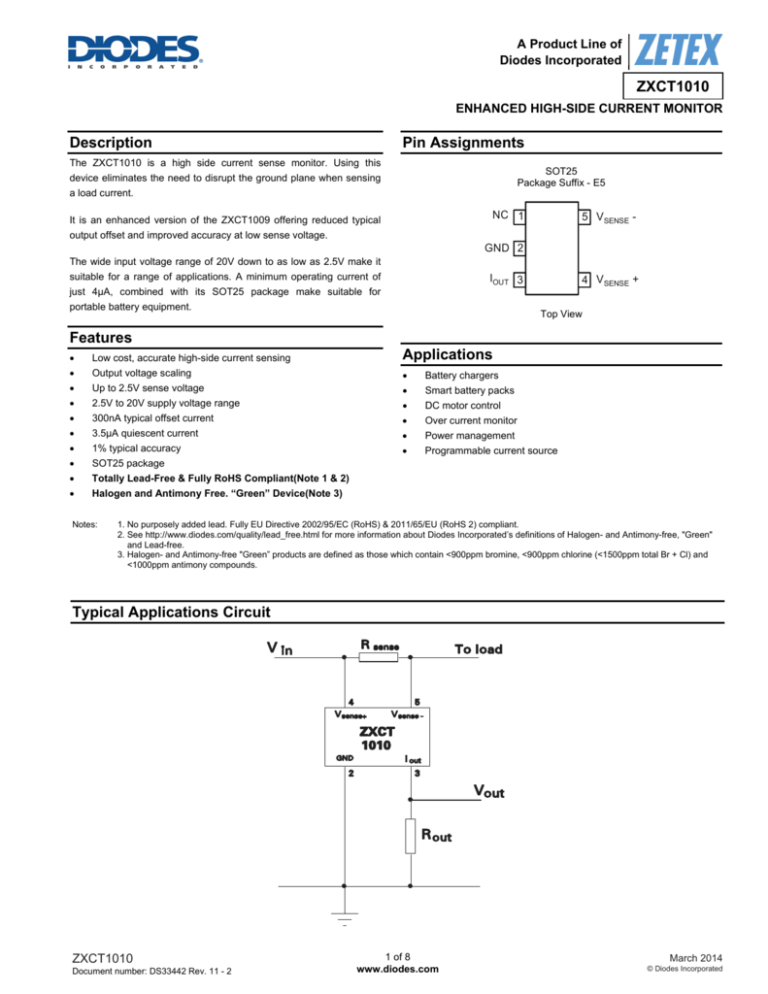
A Product Line of Diodes Incorporated ZXCT1010 ENHANCED HIGH-SIDE CURRENT MONITOR Description Pin Assignments The ZXCT1010 is a high side current sense monitor. Using this SOT25 Package Suffix - E5 device eliminates the need to disrupt the ground plane when sensing a load current. NC 1 It is an enhanced version of the ZXCT1009 offering reduced typical 5 VSENSE - output offset and improved accuracy at low sense voltage. GND 2 The wide input voltage range of 20V down to as low as 2.5V make it suitable for a range of applications. A minimum operating current of IOUT 3 just 4µA, combined with its SOT25 package make suitable for portable battery equipment. 4 VSENSE + Top View Features • Low cost, accurate high-side current sensing Applications • Output voltage scaling • Battery chargers • Up to 2.5V sense voltage • Smart battery packs • 2.5V to 20V supply voltage range • DC motor control • 300nA typical offset current • Over current monitor • 3.5µA quiescent current • Power management • 1% typical accuracy • Programmable current source • SOT25 package • Totally Lead-Free & Fully RoHS Compliant(Note 1 & 2) • Halogen and Antimony Free. “Green” Device(Note 3) Notes: 1. No purposely added lead. Fully EU Directive 2002/95/EC (RoHS) & 2011/65/EU (RoHS 2) compliant. 2. See http://www.diodes.com/quality/lead_free.html for more information about Diodes Incorporated’s definitions of Halogen- and Antimony-free, "Green" and Lead-free. 3. Halogen- and Antimony-free "Green” products are defined as those which contain <900ppm bromine, <900ppm chlorine (<1500ppm total Br + Cl) and <1000ppm antimony compounds. Typical Applications Circuit ZXCT1010 Document number: DS33442 Rev. 11 - 2 1 of 8 www.diodes.com March 2014 © Diodes Incorporated A Product Line of Diodes Incorporated ZXCT1010 Pin Descriptions Pin Number 1 2 3 Pin Name NC GND IOUT 4 VSENSE- Function No connection Ground Output current, proportional to VIN - VLOAD Supply voltage 5 VSENSE+ Connection to load/battery Functional Block Diagram Absolute Maximum Ratings (@TA = +25°C, unless otherwise specified.) Parameter Voltage on any pin (relative to IOUT) Continuous output current, IOUT Continuous sense voltage, VSENSE (Note 4) Operating temperature, TA Storage temperature Package power dissipation(@TA = +25°C) Note: Rating -0.6 to +20 25 -0.5 to +0.5 -40 to +85 -55 to +125 300 SOT25 Unit V mA V °C °C mW 4. Operation above the absolute maximum rating may cause device failure. Operation at absolute maximum ratings, for extended periods, may reduce device reliability Electrical Characteristics (@TA = +25°C, unless otherwise specified.) Symbol VIN IOUT Iq VSENSE ISENSEACC GM BW Notes: Parameter VCC range Output Current (Note 5) Ground pin current Sense Voltage (Note 6) VSENSE - Input Current Accuracy Transconductance, IOUT/VSENSE Bandwidth Conditions − VSENSE = 0V VSENSE = 10mV VSENSE = 100mV VSENSE = 200mV VSENSE = 1V VSENSE = 0V − RSENSE = 0.1Ω; VSENSE = 200mV − VSENSE(DC) = 10mV, RF PIN = -40dBm (Note 7) VSENSE(DC) = 100mV, RF PIN = -20dBm (Note 7) Min 2.5 0 85 0.975 1.95 9.7 — 0 — -2.5 — — Limits Typ − 0.3 100 1.0 2.0 10.0 3.5 — — — 10000 300 Max 20 10 115 1.025 2.05 10.3 8 2500 100 2.5 — — — 2 — Units V µA mA µA mV nA % µA/V kHz MHz 5. Include input offset voltage contribution 6. VSENSE is defined as the differential voltage between VSENSE+ and VSENSE-, VSENSE = VSENSE+ -VSENSE- =VIN-VLOAD = ILOAD * RSENSE 7. -20dBm = 63mVP-P into 50Ω ZXCT1010 Document number: DS33442 Rev. 11 - 2 2 of 8 www.diodes.com March 2014 © Diodes Incorporated A Product Line of Diodes Incorporated ZXCT1010 Typical Performance Characteristics ZXCT1010 Document number: DS33442 Rev. 11 - 2 3 of 8 www.diodes.com March 2014 © Diodes Incorporated A Product Line of Diodes Incorporated ZXCT1010 Power Dissipation The maximum allowable power dissipation of the device for normal operation (PMAX), is a function of the package junction temperature (TJ(MAX)), and ambient temperature (TAMB), according to the expression. PMAX = (TJ(MAX) – TAMB)/θJA The device power dissipation, PD is given by the expression: PD = IOUT*(VIN – VOUT) Watts Application Information The following lines describes how to scale a load current to an output voltage. VSENSE = VIN – VLOAD VOUT = 0.01 x VSENSE x ROUT E.g. A 1.0A current is to be represented by a 100mV output voltage: 1) Choose the value of RSENSE to give 50mV > VSENSE > 500mV at full load. For example, VSENSE = 100mV at 1.0A. RSENSE = 0.1/1.0 = > 0.1ohms. 2) Choose ROUT to give VOUT = 100mV, when VSENSE = 100mV. Rearranging for Rout gives: ROUT = VOUT/(VSENSE x 0.01) ROUT = 0.1/(0.1 x 0.01) = 100Ω Typical Application Circuit Typical Circuit Application: When RLOAD represented any load including DC motors, a charging battery or further circuitry that requires monitoring, RSENSE can be selected on specific requirements of accuracy, size and power rating. ZXCT1010 Document number: DS33442 Rev. 11 - 2 4 of 8 www.diodes.com March 2014 © Diodes Incorporated A Product Line of Diodes Incorporated ZXCT1010 Application Information (cont.) Li-ion Charger Circuit: The figure below shows the ZXCT1010 supporting the Benchmarq bq2954 Charge Management IC. Most of the support components for the bq2954 are omitted for clarity. This design also uses the Zetex FZT789A high current Super-b PNP as the switching transistor in the DC-DC step down converter and the FMMT451 as the drive NPN for the FZT789A. The circuit can be configured to charge up to four Li-ion cells at a charge current of 1.25A. Charge can be terminated on maximum voltage, selectable minimum current, or maximum time out, switching frequency of the PWM loop is approximately 120kHz. Bi-Directional Current Sensing: The ZXCT1010 can be used to measure current bi-directionally, if two devices are connected as show below: If the voltage V1 is positive with respect to the voltage V2 the lower device will be active, delivering a proportional output current to Rout. Due to the polarity of the voltage across RSENSE, the upper device will be inactive and will not contribute to the current delivered to Rout. When V2 is more positive than V1, current will be flowing in the opposite direction, causing the upper device to be active instead. Non-linearity will be apparent at small values of VSENSE due to offset current contribution. Devices can use separate output resistors if the current direction is to be monitored independently. ZXCT1010 Document number: DS33442 Rev. 11 - 2 5 of 8 www.diodes.com March 2014 © Diodes Incorporated A Product Line of Diodes Incorporated ZXCT1010 Application Information (cont.) Bi-Directional Transfer Function: PCB Trace Shunt Resistor for Low Cost Solution: The figure below shows output characteristics of the device when using a PCB resistive trace for a low cost solution in replacement for a conventional shunt resistor. The graph shows the linear rise in voltage across the resistor due to the PTC of the material and demonstrates how this rise in resistance value over temperature compensates for the NTC of the device. The figure opposite shows a PCB layout suggestion. The resistor section is 25mm x 0.25mm giving approximately 150mΩ using 1oz copper. The data for the normalized graph was obtained using a 1A load current and a 100Ω output resistor. An electronic version of the PCB layout is available by request. ZXCT1010 Document number: DS33442 Rev. 11 - 2 6 of 8 www.diodes.com March 2014 © Diodes Incorporated A Product Line of Diodes Incorporated ZXCT1010 Ordering Information Part Number ZXCT1010E5TA Note: Reel Size 7” Tape Width 8mm Quantity per Reel 3000 Units Part Marking 101 Package SOT25 8. Pad layout as shown on Diodes Inc. suggested pad layout document AP02001, which can be found on our website at http://www.diodes.com/datasheets/ap02001.pdf Package Outline Dimensions (All dimensions in mm.) Please see AP02002 at http://www.diodes.com/datasheets/ap02002.pdf for latest version. A SOT25 Dim Min Max Typ A 0.35 0.50 0.38 B 1.50 1.70 1.60 C 2.70 3.00 2.80 D ⎯ ⎯ 0.95 H 2.90 3.10 3.00 J 0.013 0.10 0.05 K 1.00 1.30 1.10 L 0.35 0.55 0.40 M 0.10 0.20 0.15 N 0.70 0.80 0.75 0° 8° α ⎯ All Dimensions in mm B C H K M N J L D Suggested Pad Layout Please see AP02001 at http://www.diodes.com/datasheets/ap02001.pdf for latest version. C2 Z C2 Dimensions Value (in mm) Z 3.20 G 1.60 X 0.55 Y 0.80 C1 G C1 C2 Y 2.40 0.95 X ZXCT1010 Document number: DS33442 Rev. 11 - 2 7 of 8 www.diodes.com March 2014 © Diodes Incorporated A Product Line of Diodes Incorporated ZXCT1010 IMPORTANT NOTICE DIODES INCORPORATED MAKES NO WARRANTY OF ANY KIND, EXPRESS OR IMPLIED, WITH REGARDS TO THIS DOCUMENT, INCLUDING, BUT NOT LIMITED TO, THE IMPLIED WARRANTIES OF MERCHANTABILITY AND FITNESS FOR A PARTICULAR PURPOSE (AND THEIR EQUIVALENTS UNDER THE LAWS OF ANY JURISDICTION). Diodes Incorporated and its subsidiaries reserve the right to make modifications, enhancements, improvements, corrections or other changes without further notice to this document and any product described herein. Diodes Incorporated does not assume any liability arising out of the application or use of this document or any product described herein; neither does Diodes Incorporated convey any license under its patent or trademark rights, nor the rights of others. Any Customer or user of this document or products described herein in such applications shall assume all risks of such use and will agree to hold Diodes Incorporated and all the companies whose products are represented on Diodes Incorporated website, harmless against all damages. Diodes Incorporated does not warrant or accept any liability whatsoever in respect of any products purchased through unauthorized sales channel. Should Customers purchase or use Diodes Incorporated products for any unintended or unauthorized application, Customers shall indemnify and hold Diodes Incorporated and its representatives harmless against all claims, damages, expenses, and attorney fees arising out of, directly or indirectly, any claim of personal injury or death associated with such unintended or unauthorized application. Products described herein may be covered by one or more United States, international or foreign patents pending. Product names and markings noted herein may also be covered by one or more United States, international or foreign trademarks. This document is written in English but may be translated into multiple languages for reference. Only the English version of this document is the final and determinative format released by Diodes Incorporated. LIFE SUPPORT Diodes Incorporated products are specifically not authorized for use as critical components in life support devices or systems without the express written approval of the Chief Executive Officer of Diodes Incorporated. As used herein: A. Life support devices or systems are devices or systems which: 1. are intended to implant into the body, or 2. support or sustain life and whose failure to perform when properly used in accordance with instructions for use provided in the labeling can be reasonably expected to result in significant injury to the user. B. A critical component is any component in a life support device or system whose failure to perform can be reasonably expected to cause the failure of the life support device or to affect its safety or effectiveness. Customers represent that they have all necessary expertise in the safety and regulatory ramifications of their life support devices or systems, and acknowledge and agree that they are solely responsible for all legal, regulatory and safety-related requirements concerning their products and any use of Diodes Incorporated products in such safety-critical, life support devices or systems, notwithstanding any devices- or systems-related information or support that may be provided by Diodes Incorporated. Further, Customers must fully indemnify Diodes Incorporated and its representatives against any damages arising out of the use of Diodes Incorporated products in such safety-critical, life support devices or systems. Copyright © 2014, Diodes Incorporated www.diodes.com ZXCT1010 Document number: DS33442 Rev. 11 - 2 8 of 8 www.diodes.com March 2014 © Diodes Incorporated
