AN-771
APPLICATION NOTE
One Technology Way • P.O. Box 9106 • Norwood, MA 02062-9106 • Tel: 781/329-4700 • Fax: 781/461-3113 • www.analog.com
ADSP-BF533 EZ-KIT Lite® and ADF70xx Interface
by Austin Harney and Regis Guillermin
This application note explains how to quickly interface
the ADF70xx transceiver board with the EZ-KIT board.
CONNECTIONS
• USB cable (type A to B) between the host computer
and the EZ-KIT board
HARDWARE DESCRIPTION
•
EZ-KIT power supply (7.5 V dc/~2 A)
SOFTWARE DESCRIPTION
• VisualDSP++ ® (v3.5) with license or 90 - day free
test drive
•
•
EZKIT-70xx_interface.zip code file
USB drivers
Analog Devices software and processor manuals are
available at the following links:
Blackfin® Processor
http://www.analog.com/processors/processors/blackfin/
index.html
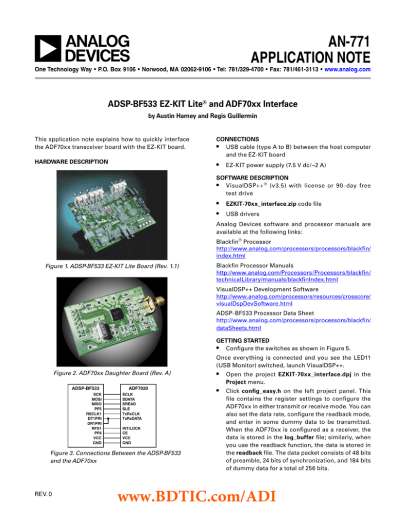
Figure 1. ADSP-BF533 EZ-KIT Lite Board (Rev. 1.1)
Blackfin Processor Manuals
http://www.analog.com/Processors/Processors/blackfin/
technicalLibrary/manuals/blackfinIndex.html
VisualDSP++ Development Software
http://www.analog.com/processors/resources/crosscore/
visualDspDevSoftware.html
ADSP-BF533 Processor Data Sheet
http://www.analog.com/processors/processors/blackfin/
dataSheets.html
GETTING STARTED
• Configure the switches as shown in Figure 5.
Once everything is connected and you see the LED11
(USB Monitor) switched, launch VisualDSP++.
Figure 2. ADF70xx Daughter Board (Rev. A)
ADSP-BF533
SCK
MOSI
MISO
PF5
RSCLK1
DT1PRI
DR1PRI
RFS1
PF6
VCC
GND
ADF7020
SCLK
SDATA
SREAD
SLE
TxRxCLK
TxRxDATA
INT/LOCK
CE
VCC
GND
Figure 3. Connections Between the ADSP-BF533
and the ADF70xx
REV. 0
•
Open the project EZKIT-70xx_interface.dpj in the
Project menu.
•
Click config_easy.h on the left project panel. This
file contains the register settings to configure the
ADF70xx in either transmit or receive mode. You can
also set the data rate, configure the readback mode,
and enter in some dummy data to be transmitted.
When the ADF70xx is configured as a receiver, the
data is stored in the log_buffer file; similarly, when
you use the readback function, the data is stored in
the readback file. The data packet consists of 48 bits
of preamble, 24 bits of synchronization, and 184 bits
of dummy data for a total of 256 bits.
www.BDTIC.com/ADI
AN-771
•
•
Figure 4 shows the different modes with switches that
you can use.
Next you can build the project using the Rebuild
All command in the Project menu. The compilation
should be completed successfully and load the code
into the board.
To run the program, click Run on the Debug menu.
The LED4 should be on.
LED4 ON
LED4 OFF
SW4 = READBACK
RUN
Choose the mode. The program is a loop, so when
LED4 reappears the mode is finished, and you can
choose the mode again, and so on. To check if it’s
working or not, probe the INT/LOCK pin (Pin 7) on
the receive side to know if the synchronization word
is detected.
SW5 = Tx MODE
AN05391–0–3/05(0)
•
SW6 = Rx MODE
SW7 = END
Figure 4. Usable Modes with Switches
Figure 5. Switch Default Configuration
SW4 = Readback
SW5 = Tx mode
SW6 = Rx mode
SW7 = End
LED4 On = Idle state, waiting for a mode
Figure 6.
LED4 Off = Busy state
www.BDTIC.com/ADI
© 2005 Analog Devices, Inc. All rights reserved. Trademarks and registered trademarks are the property of their respective owners.
–2–
REV. 0
