Induced electrical polarization is a powerful tool to modify and
advertisement
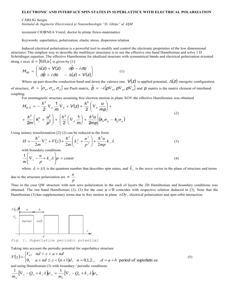
ELECTRONIC AND INTERFACE SPIN STATES IN SUPERLATTICE WITH ELECTRICAL POLARIZATION CÂRLIG Sergiu Insitutul de Inginerie Electronică şi Nanotehnologii “D. Ghiţu” al AŞM recenzent CIORNEA Viorel, doctor în ştiinţe fizico-matematice Keywords: superlattice, polarization, elastic stress, dispersion relation Induced electrical polarization is a powerful tool to modify and control the electronic proprieties of the low dimensional structures. The simplest way to describe the multilayer structures is to use the effective one band Hamiltonian and solve 1 D Schrödinger equation. The effective Hamiltonian for idealized structure with symmetrical bands and electrical polarization oriented along z axes u 0,0, u is given by [1]: H 00 ˆ z V z p i u ˆ p i u z V z (1) V z is applied potential, z energetic configuration ̂ of structure, x , y , z are Pauli matrix, p i p x , p y , p z and p matrix is the matrix element of interband Where up part describe conduction band and down the valence one. coupling. For nonmagnetic structure assuming free electron motion in plane XOY the effective Hamiltonian was obtained H 2 2 2 1 2 u z z z V z 2 m 2 mp (2) 2 2 u2 2 1 2u k 2 z kx y ky x 2m m 2mp p 2 Using unitary transformation [2] (2) can be reduced to the form: H 2 2 2 2 u 2 2u k 2 z V z k 2m 2m p 2mp (3) with boundary conditions 1 u z k const m p where (4) 1 is the quantum number that describes spin states, and k due to the structure polarization are is the wave vector in the plane of structure and terms u . p Thus in the case QW structure with non zero polarization in the each of layers the 2D Hamiltonian and boundary conditions was obtained. The one band Hamiltonian (2), (3) for the case u 0 coincides with respective relation deduced in [3]. Note that the Hamiltonian (3) has supplementary terms due to free motion in plane xOy , electrical polarization and spin orbit interaction. V z a b barrier well V0 z d fig. 1. Superlatice periodic potential Taking into account the periodic potential for superlattice structure V , nd z a nd V z 0 0, a nd z n 1d , n 0,1,2... d a b period of superlatti ce and using Hamiltonian (3) with boundary / periodic conditions 1 z Qw k w 1 z Qb k b mw mb (5) 1 z Qw k w 0e iqd 1 z Qb k b d mw mb (6) w 0e iqd b d w b b b we obtain the relation of dispersion of such structure. A sin b sinh ak B cos b cosh ak B cos qd A k Qb Qw k 1 2 2 2 (7) 2 (8) B 2k (9) with wave vector in barrier and well given by: 2mb V0 E 2 k Qb 2 k (10) 2mw E 2 k Qw 2 (11) For evanescent electron behaviour near to interface between layers ( w e z ) electronic interface states [4] are given by dispersion relation: A sinh b sinh ak B cosh b cosh ak B cos qd (12), where A k 2 Qb Qw k 1 2 2 2 (13) B 2k (11) 2mb V0 E 2 k Qb 2 k (14) 2mw E 2 k Qw 2 (15) In (2-15) the notations are the following: 1 is the quantum number that describes spin states, and k is the wave vector in the u plane of structure and terms due to the structure polarization are Q . Index “w” and “b” are assigned to well and barrier p structures respectively. The terms due to elastic stress Q w ,b and free motion in the xOy plane (z axis is the growth axes of the structure) lead to effective potential given by: Veff 2 2 2 k 2 Qw Qw k k 2 Qb Qb k V z 2 mw mb (16) k k the well disappear and for k k the well "became" barrier. Critical wave vector in the perpendicular direction can be obtained from condition Veff 0 and it is expressed as: For critical value of k cr Qb Qw c c 4 1 Qb2 2mwV0 2 Qw2 Qb Qw 2 2 1 2 (17) fig. 2. Critical values of k cr for 1, 2, mw 0,07 me ,V0 150 meV Electronic quantum dimensional and interface states are plotted for different values of parameters of structure, includes thickness of layers, elastic stress, mass ratio. Elastic stresses are assumed for 4 cases: with opposite sign, with same sign and null in one or other layer. For small period of superlatice there is a perceptible difference between spin up and spin down electronic states. Interface states appear for energies greater than height of superlatice barrier. In all case, distinction between spineless electron and electrons with spin up or down disappear with increasing of thickness of layers and / or with growing of mass ratio. fig. 3 a Elastic stress with opposite sign fig. 3 b. Elastic stress with same signs in layers fig. 3 c. Increasing of mass ratio, and thickness of layers implies small differences between spin states of electrons fig. 4 a. Elastic stress in the barrier layer is zero. fig 4 b. Increasing of mass ratio, and thickness of layers implies small differences between spin states of electrons Acknowledgemnts The financial support of the major researches of this work is in the frame of project no 5390 STCU. References [1] S.Cârlig, F.Ermalai, V.Kantser Polarization induced topological states in semiconductor layered structures, abstracts of physicist conference of Moldova 2009, pg 63 [2] G. Bîrliba, S. Carlig and V. Kantser, Spin-orbit interaction and electronic states in semiconductor quantum structures, Proceedings of Fifth General Conference of the Balkan Physical Union, 2003 [3] A. V. Kolesnikov and A. P. Silin, Phys. Rev. B 59, 7596 (1999) [4] N.Malkova, U. Ekenberg, Spin properties of quantum wells with magnetic barriers. II. Inverted band ordering and spin polarized interface states Phys. Rev. B 66, 155325 (2002)
