doc
advertisement

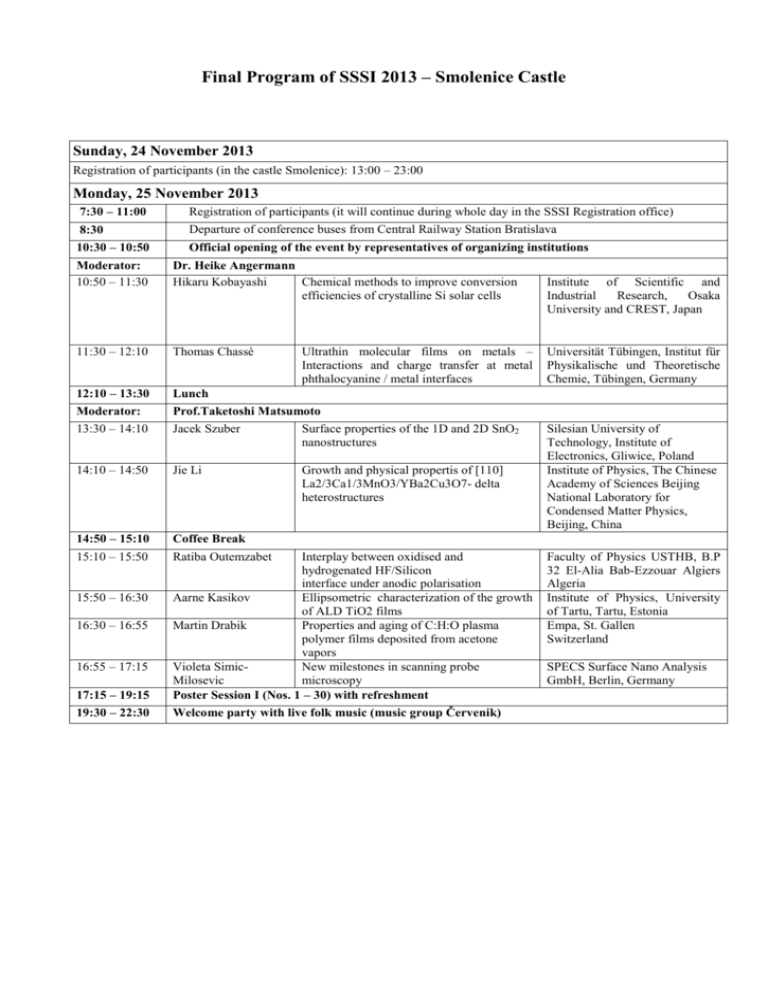
Final Program of SSSI 2013 – Smolenice Castle Sunday, 24 November 2013 Registration of participants (in the castle Smolenice): 13:00 – 23:00 Monday, 25 November 2013 7:30 – 11:00 Registration of participants (it will continue during whole day in the SSSI Registration office) 8:30 Departure of conference buses from Central Railway Station Bratislava 10:30 – 10:50 Official opening of the event by representatives of organizing institutions Moderator: 10:50 – 11:30 Dr. Heike Angermann Hikaru Kobayashi Chemical methods to improve conversion efficiencies of crystalline Si solar cells 11:30 – 12:10 Thomas Chassé 12:10 – 13:30 Lunch Moderator: Prof.Taketoshi Matsumoto 13:30 – 14:10 Jacek Szuber Surface properties of the 1D and 2D SnO2 nanostructures 14:10 – 14:50 Jie Li Growth and physical propertis of [110] La2/3Ca1/3MnO3/YBa2Cu3O7- delta heterostructures 14:50 – 15:10 Coffee Break 15:10 – 15:50 Ratiba Outemzabet Ultrathin molecular films on metals – Interactions and charge transfer at metal phthalocyanine / metal interfaces 17:15 – 19:15 Interplay between oxidised and hydrogenated HF/Silicon interface under anodic polarisation Aarne Kasikov Ellipsometric characterization of the growth of ALD TiO2 films Martin Drabik Properties and aging of C:H:O plasma polymer films deposited from acetone vapors Violeta SimicNew milestones in scanning probe Milosevic microscopy Poster Session I (Nos. 1 – 30) with refreshment 19:30 – 22:30 Welcome party with live folk music (music group Červeník) 15:50 – 16:30 16:30 – 16:55 16:55 – 17:15 Institute of Scientific and Industrial Research, Osaka University and CREST, Japan Universität Tübingen, Institut für Physikalische und Theoretische Chemie, Tübingen, Germany Silesian University of Technology, Institute of Electronics, Gliwice, Poland Institute of Physics, The Chinese Academy of Sciences Beijing National Laboratory for Condensed Matter Physics, Beijing, China Faculty of Physics USTHB, B.P 32 El-Alia Bab-Ezzouar Algiers Algeria Institute of Physics, University of Tartu, Tartu, Estonia Empa, St. Gallen Switzerland SPECS Surface Nano Analysis GmbH, Berlin, Germany Tuesday, 26 November 2013 7:30 – 8:30 Breakfast Moderator: 8:30 – 9:10 Prof. Alexander Šatka D.R.T. Zahn Growth and Doping of Ultrathin Semiconducting Molecular Films 9:10 – 9:50 Heike Angermann 9:50 – 10:10 Coffee Break 10:10 – 10:50 Zsolt J. Horváth Simulation - tool for understanding memory behaviour of non-volatile structures 10:50 – 10:15 Daniel Haško 11:15 – 11:40 Tomasz Giela Atomic force microscopy investigations of amorphous ZnO layers grown by pulsed laser deposition. The investigation of high temperature tungsten oxide phases and their transitions with LEEM microscopy 11:40 – 12:05 Marián Marton Nanostructuring of diamond thin films by DC and RF plasma etching 12:05 – 12:25 Mamadou Seck Characterization of the degradation process of Si-PCPDTBT:PC70BM(1:2) bland layers deposited on ITO/glass substrate 12:25 – 13:30 Conditioning of Silicon substrates by wetchemical etching and oxidation Semiconductor Physics Research Group, Chemnitz University Technology, Physics Department / Semiconductor Physics, Chemnitz, Germany Helmholtz-Zentrum, Institut für Silizium-Photovoltaik,Berlin, Germany Obuda University, Kando Kalman Faculty of Electrical Engineering, Institute of Microelectronics and Technology, Budapest, Hungary International Laser Centre, Bratislava, Slovakia Jerzy Haber Institute of Catalysis and Surface Chemistry, Polish Academy of Sciences Kraków, Poland Faculty of Electrical Engineering and Information Technology, Slovak University of Technology, Bratislava, Slovakia International Laser Centre, Bratislava, Slovakia Lunch Moderator: Prof. Ladislav Harmatha 13:30 – 13:55 Roman Ďurikovič Modelling the Spectral BRDF Based on the Spectral Measurements of Metallic Paints 13:55 – 14:20 Anatoli Evtukh 14:20 – 14:45 Stanislav Jurečka Enhanced Field Emission Current due to Reconstruction of the Nanosize Carbon Cathodes Investigation of tunneling current in MOS devices with ultrathin gate oxide 14:45 – 15:10 Jaroslav Kováč 15:10 – 15:35 Emil Pincik 15:35 – 15:55 15:55 – 16:20 Coffee break Vladimyr Litovchenko 16:20 - 16:45 Bohuslav Rezek 16:45 – 17:10 Jiří Vondrák 17:10 – 17:30 Martin Schaefer 17:30 – 19:30 Poster session II (Nos. 31 – 60) with refreshment Study of ZnO nanoclusters grown by a hydrothermal process on GaP/ZnO nanowires About optical properties of black silicon Enhanced Field Emission Current due to Reconstruction of the Nanosize Carbon Cathodes Microscopic morphology of epithelial cells on functionalized diamond and glass Capacity of carbon electrode in aprotic anhydrous solvents Company presentation Faculty of Mathematics, Physics and Informatics, Comenius University, Bratislava, Slovakia V. Lashkaryov Institute of Semiconductor Physics, Kiev, Ukraine Institute of Aurel Stodola, FEE University of Žilina, Liptovský Mikuláš, Slovak Republic Institute of Electronics and Photonics, Slovak University of Technology, Bratislava, Slovakia Institute of Physics SAS, Bratislava, Slovakia V. Lashkaryov Institute of Semiconductor Physics, Kiev, Ukraine Institute of Physics ASCR, Prague, Czech Republic Department of Electrotechnology FEEC VUT Brno, Czech Republic Schaefer Technologie GmbH; Langen, Deutschland and Kvant s.r.o., Bratislava, Slovakia 19:30 – 21:30 Conference dinner in suitable representative spaces of the castle 15:30 – 23:30 Visit of Opera in Slovak National Theatre, Bratislava: opera of Giuseppe Verdi Wednesday, 27 November 2013 7:30 – 8:30 Breakfast Moderator: 8:30 – 9:10 Prof. Thomas Chassé Yossi Paltiel Surface proximity effects in hybrid superconductor/organiclinker/nanoparticle systems 9:10 – 9:50 Grzegorz Jung 9:50 – 10:10 Universal crackling charge dynamics on semiconducting surfaces covered with 2D molecular layers. Coffee break 10:10 – 10:50 Andrej Pleceník Gas sensors based on TiO2 thin films 10:50 – 11:30 Ikuta Hiroshi Study of Thin Film Growth of Iron Based Superconductors and Their Characterization 11:30 – 11:55 Jozef Novák Columnar microstructure of the ZnO shell nanowire layer 11:55 – 12:20 Alexander Kromka Diamond Growth on Germanium as Chemically and Temperature Sensitive Substrate 12:20 – 13:30 School of Engineering and Computer Science, Faculty of Science, The Hebrew University,Jerusalem, Israel Ben Gurion University of the Negev, Beer Sheva, Israel FMPI Comenius University, Bratislava, Slovakia Department of Crystalline Materials Science, Nagoya University, Nagoya, Japan Institute of Electrical Engineering, Slovak Academy of Sciences, Bratislava, Slovak Republic Institute of Physics of the ASCR,v.v.i., Praha, Czech Republic Lunch Moderator: Prof. Dietrich R. T. Zahn 13:30 – 14:10 Miikhail Belogolovskii 14:10 – 14:50 Maeda Atsutaka 14:50 – 15:10 15:10 – 15:50 Coffee break Iida Kazumasa 15:50 – 16:30 Daghero Dario 16:30 – 16:55 Marián Trgala 16:55 – 17:20 Michał Ślęzak 17:20 – 19:20 Poster session III (Nos. 61 – 90), with refreshment 19:30 – 21:30 Informal working meeting with dinner in spaces of the castle – e.g. in Jaeger Saloon Testing the universality aspects of charge transport accross ultra-thin disordered insulating layers Synthesis of high-quality epitaxial thin films of Fe-chalcogenides superconductor and its physical properties Donetsk Institute for Physics and Engineering, Donetsk, Ukraine Generic Fe-buffer layers for epitaxial Febased superconducting thin films Advanced surface characterization of Codoped Ba-122 thin films and fundamental study of their properties by point contact and transport measurements Superconducting MoC thin films for coplanar waveguide resonators IFW Dresden, Germany Prospects of X-ray Photoemission Electron Microscopy at the first beamline of Polish synchrotron SOLARIS Department of Basics Sciences, University of Tokyo, Komaba, Tokyo, Japan Dipartimento di Scienza Applicata e Tecnologia (DISAT) Politecnico di Torino, Italy Department of Experimental Physics, FMPI, Comenius University, Bratislava, Slovakia 1. Swiss Light Source, Paul Scherrer Institut, Switzerland 2. Faculty of Physics and Applied Computer Science, AGH, Kraków, Poland Thursday, 28 November 2013 7:30 – 8:30 Breakfast Moderator: 8:30 – 9:10 Prof. Jacek Szuber Taketoshi Matsumoto 9:10 – 9:50 Pavel Tomanek 9:50 – 10:10 10:10 – 10:50 Coffee Break Štefan Chromik 10:50 – 11:30 Peter Švec 11:30 – 11:55 Tomáš Pleceník 11:55 – 12:20 Necmettin Kilinc 12:20 – 12:30 Conclusion 12:30 – 14:00 Lunch 14:00 Conference bus departure to Bratislava (Central bus station and Central railway station) 16:00 – 19:00 Excursion to Labs of Faculty of Mathematics, Physics, and Informatics of Comenius University in Bratislava Nitric acid oxidation of Si (NAOS) method for application to thin film transistors (TFT), eternal memory “digital Rosetta Stone”, and Si solar cells Microstructure defect types in silicon solar cells Institute of Scientific and Industrial Research, Osaka University, Osaka, Mihogaoka, Ibaraki, Japan 1) Brno University of Technology, FEEC, Czech Republic 2) South Dakota School of Mines and Technology, Rapid City, SD, USA LSMO thin films with high metal- insulator transition temperature on buffered SOI substrates for uncooled microbolometers Phase and orientation mapping of finegrained structures by precession electron diffraction Surface transport properties and degradation of Fe-based superconductors Institute of Electrical Engineering, Slovak Academy of Sciences, Bratislava, Slovakia Institute of Physics SAS, Bratislava, Slovakia Electrical and structural characteristics of TiO2 nanotube - MPc heterojuctions Department of Experimental Physics, Faculty of Mathematics, Physics and Informatics, Comenius University, Bratislava Slovakia Gebze Institute of Technology, Science Faculty, Department of Physics, Gebze-Kocaeli, Turkey

