Example No
advertisement
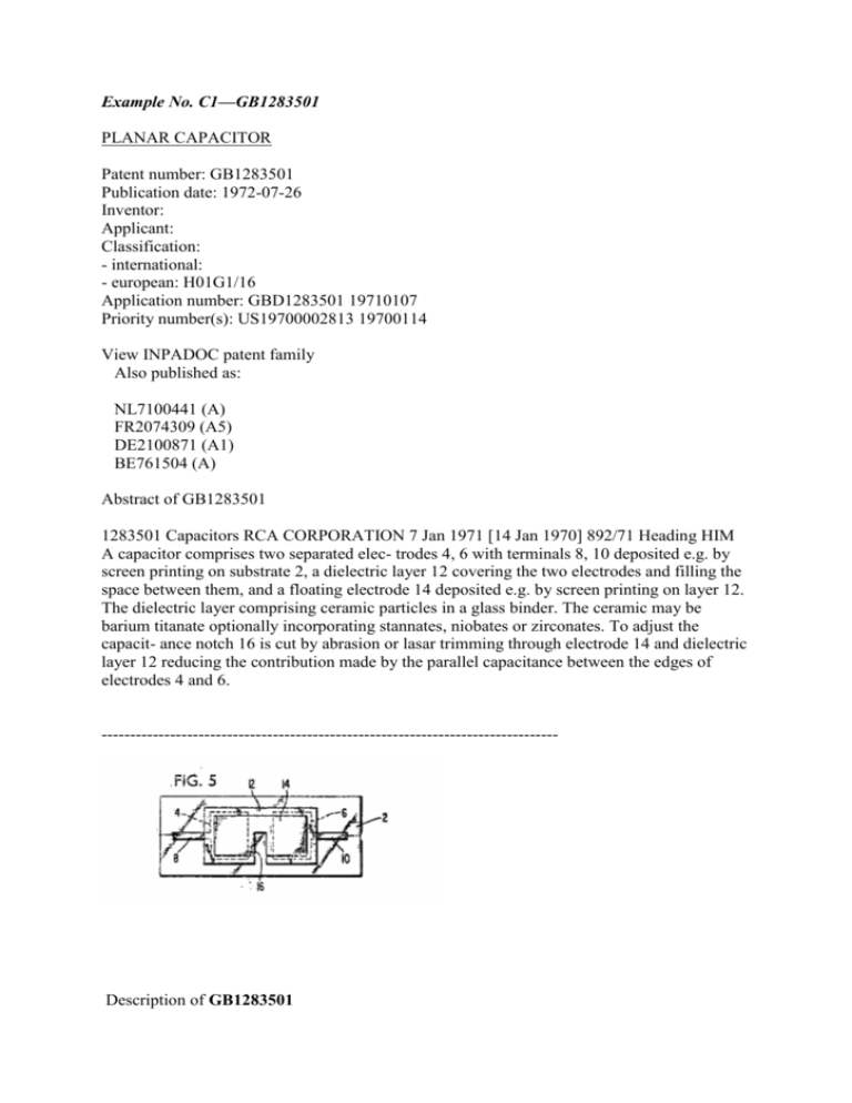
Example No. C1—GB1283501 PLANAR CAPACITOR Patent number: GB1283501 Publication date: 1972-07-26 Inventor: Applicant: Classification: - international: - european: H01G1/16 Application number: GBD1283501 19710107 Priority number(s): US19700002813 19700114 View INPADOC patent family Also published as: NL7100441 (A) FR2074309 (A5) DE2100871 (A1) BE761504 (A) Abstract of GB1283501 1283501 Capacitors RCA CORPORATION 7 Jan 1971 [14 Jan 1970] 892/71 Heading HIM A capacitor comprises two separated elec- trodes 4, 6 with terminals 8, 10 deposited e.g. by screen printing on substrate 2, a dielectric layer 12 covering the two electrodes and filling the space between them, and a floating electrode 14 deposited e.g. by screen printing on layer 12. The dielectric layer comprising ceramic particles in a glass binder. The ceramic may be barium titanate optionally incorporating stannates, niobates or zirconates. To adjust the capacit- ance notch 16 is cut by abrasion or lasar trimming through electrode 14 and dielectric layer 12 reducing the contribution made by the parallel capacitance between the edges of electrodes 4 and 6. -------------------------------------------------------------------------------- Description of GB1283501 (54) PLANAR CAPACITOR (71) We, RCA CORPORATION, a corporation organised under the laws of the State of Delaware, United States of America, of 30 Rockefeller Plaza, City and State of New York, United States of America, do hereby declare the invention, for which we pray that a patent may be granted to us, and the method by which it is to be performed, to be particularly described in and by the followingstatement: Thick film hybrid integrated circuits have generally used capacitors in the form of discrete ceramic chips provided with metal film electrodes, mounted on a substrate which has a pattern of conductors printed thereon. Although these circuits have had widespread commercial acceptance, the cost of handling and mounting these discrete components is relatively high. To reduce manufacturing costs, capacitors have also been made byscreen-printing successive layers of metal compositions, and dielectric compositions on the substrate. These have been successful for relatively large values of capacitance. But for low values of capacitance (i.e., less than about 100 picofarads), they have many disadvantages. For low values of capacitance, the conventional screened-on type capacitor becomes undesirably small. The screen-printing of layers of metal compositions and of dielectric compositions is not a precision operation. Small variations of thickness of coating and of shape readily occur and these can cause relatively large percentage changes in capacitance of a low value capacitor.Conventional trimming with an abrasive jet to adjust the value of a screen-printed capacitor to a required value also become impossible when the size of the capacitor becomes too small. And, even when the capacitor is large enough to be trimmed, the abrasive action often drags metal from the top electrode over the cut edge to short out the bottom electrode. Ceramic chip type capacitors can be made with precise values of capacitance but, for low values of capacitance, these have a disadvantage other than higher cost The metal film connection from the top electrode to a conductor printed on a substrate must pass over a sharp edge. It is difficult to screenprint this connection without a high percentage of breaks in the film. Moreover, the metal film introduced additional capacitance into the circuit. An object of the present invention is to provide an improved capacitor of the screenprinted type which is particularly adapted for low values of capacitance. A furrher object of the invention is to provide a screen-printed, low-value, capacitor that can readily be adjusted in value by trimming. According to the invention we provide a capacitor characterized by comprising: two metal film electrodes separated by a predetermined distance and disposed on an insulating substrate, said electrodes being adapted to be electrically connected into a circuit, a layer of dielectric insulating material at least partially covering said two electrodes and the space therebetween, and, a third metal film electrode, not adapted to be connected in circuit, disposed on said layer of insulating material and overlapping said two electrodes said dielectric insulating material being primarily ceramic particles in a glass binder. In the accompanying drawing: FIGURES 1-3 are top plan views illustrating successive steps in manufacturing a capacitor of the present invention; FIGURE 4 is a cross-section view taken along the line 4-4 of FIGURE 3; FIGURE 5 is a top plan view of the capacitor of FIGURE 3 illustrating how its value may be adjusted by trimming; and FIGURE 6 is a cross-section view taken along the line 6-6 of FIGURE 5. EXAMPLE A capacitor in accordance with the invention can be made as follows. First, there is provided an insulating substrate 2 which may be an alumina ceramic. Then, two metallic electrodes 4 and 6, separated by a distance, of, for example 0.635 mm. are screen-printed on the substrate 2. These electrodes may have a thickness of 12.7 microns and each may be rectangular in shape with area dimension of 0.25 mm. by 5 mm., for example. Connector film leads8 and 10, connected to electrodes 4 and 6, respectively, are deposited at the same time as the electrodes. The screening composition may, for example, comprise by weight, 15.68% palladium powder,41.550/0 silver powder, 2.35% lead borosilicate glass powder,11.70% bismuth trioxide, 16% glycerol ester of hydrogenated rosin,2 nitrocellulose, and 10.72% butyl carbitol acetate blended on a 3-roll paint mill. The metal powders may have an average particle size of 2-5 microns. The particular metalizing composition used will vary depending on the dielectric material selected. The two materials must be chemically compatible. After screening, the above composition is dried at about1000--1500 C. and fired at about9009 C. The entire time in the furnace from room temperature to maximum and back to room temperature is about 40 minutes. The next step is to deposit a layer of dielectric insulating material 12 over the bottom electrodes 4 and 6 (FIGURE 2). This layer is preferably put down by screening on two or more thin films of the composition to avoid pin holes which might otherwise extend entirely through the film. Each coat is dried before the next is deposited. The layer 12 extends beyond the edges of the electrodes 4 and 6 and may have a dry thickness, overlying the bottom electrodes 4 and 6, of 50 to 75 microns. This layer is also dried at about10001500 C. The dielectric composition is not critical but may comprise primarily one or more alkaline earth metal titanates with or without one or more stannates, niobates or zirconates, a glass frit, suitable resins and a solvent such as butyl carbitol acetate. On top of the dried but still unfired dielectric layer 12 is deposited a single metal electrode 14 (FIGURE 3) dimensioned so that it overlies almost the entire area of the bottom electrodes 4 and 6 but is not quite as large in area as the sum of the areas of the two bottom electrodes as the space between them. This is to allow for registration error in manufacturing without affecting the value of the capacitance. In the capacitor of this Example, the top metal electrode was 4.5 mm. wide by 5.2 mm. long. The composition of the top electrode can be the same as the bottom electrode, or formulated separately to provide compatability of the fired composite. The top electrode is floating. It has no connection to any part of the circuit. The next step is to fire the assembly at a temperature of about8500 C. to 10500C. As in the first firing operation, the time from entering the oven at room temperature to leaving it again at room temperature is 40 minutes. The capacitor of this Example had a capacitance of 75.34 picofarads. A series of capacitors made on the same substrate and using the same materials, drying conditions and firing conditions as the capacitor of the above Example had capacitance values as shown in the table below. TABLE EMI3.1 <tb> <SEP> - <SEP> <tb> <SEP> Bottom <SEP> Electrode <SEP> Top <tb> Capacitor <SEP> Electrode <SEP> Separation <SEP> Electrode <SEP> Capaci <tb> <SEP> No. <SEP> Dimensions <SEP> Distance <SEP> Dimensions <SEP> tance <tb> 12.54 mm X0.635 mm 5.842mm x95.75pf 6.35 mm 5.207 mm 2 1.27 mmx 1.905 mm 2.286 mm x 18.75pf 2.54 mm 3.937 mm 3 1.27 mm x 1.397 mm 2.286mmx 18.47of 2.54 mm 3.429 mm 4 2.54 mm 0.635 mm 3.302 mm x 53.80of 3.81 mm 5.207 mm 51.27mum, 1.016 mm 2.286 mmx 18.95pf 2.54 mm 3.048 mm 6 2.54mm x0.635 mm 2.286mmx 38.92pf 2.54 mm 5.207 mm 7 1.27 mm x 0.635 mm 2.286 mm x17.73of 2.54 mm 2.667 mm In capacitors of the present invention, the total capacitance is a composite of three individual capacitances. Two of these are between each of the bottom electrodes 4 and 6 and the top electrode 14. These two capacitances are in series. The third is laterally between the edges of the two bottom electrodes 4 and 6. This capacitance is in parallel with the other two and is usually considerably less than either the other two. Capacitors of the present invention can readily be adjusted in value by abrasive or laser trimming without danger of shorting the electrodes or of over-trimming small value units. As shown in FIGURES 5 and 6, a notch 16 can be cut through top electrode 16 and dielectric layer 14 in the space between electrodes 4 and 6. The cutting of the notch causes air to be substituted as a dielectric for the solid composition removed, so that the capacitance between the electrodes 4 and 6 is reduced. The reduction in capacitance depends upon the length and width of the removed portion. The notch is cut only about half way across the top electrode 14 since sufficient connection between the two halves of this electrode must be left intact. It will be apparent that the amount of adjustment that can be accomplished in this manner is limited since it can only be a part of the capacitance contributed by that portion of the device between the edges of electrodes 4 and 6 and this capacitance is only a minor part of the total capacitance to begin with. Maximum adjustment possible in this manner is about 20%. Trimming adjustments are more accurate with capacitors of the present invention than with other types such as ceramic chip capacitors or conventional screen-on capacitors because the present capacitors occupy about four times as much substrate area as these other type capacitors for a given value of capacitance. Of course, where space is at a premium, this is a disadvantage. But, where space is not too important, the advantages of more accurate trimming and safer trimming without danger of shorting, are controlling. -------------------------------------------------------------------------------- Claims of GB1283501 WHAT WE CLAIMIS:1. A capacitor comprising two metal film electrodes separated by a predetermined distance and disposed on an insulating substrate, said electrodes being adapted to be electrically connected into a circuit, a layercf dielectric insulating material at least partially covering said two electrodes and the space therebetween, and, a third metal film electrode, not adapted to be connected in circuit, disposed on said layer of insulating material and overlapping said two electrodes, said dielectric insulating material being primarily ceramic particles in a glass binder. 2. A method of making a capacitor comprising: depositing at first two spaced metal film electrodes, each having circuit connection means, on an insulating substrate, covering said electrodes and the space between electrodes with a screened-on layer of dielectric insulating material of ceramic particles in a glass binder, and then depositing a third metal film electrode on said insulating layer overlapping said first two electrodes. 3. A method according to claim 2 including the further steps of: measuring the capacitance of the completed capacitor, and adjusting the capacitance to a desired value by removing a portion of said dielectric layer between said first two electrodes and the portion of said third electrode overlying the removed dielectric layer portion. 4. A method according to claim 3 wherein said dielectric layer portion and overlying metal film are removed with a stream of abrasive. 5. A method according to claim 3 in which said first two metal film electrodes are deposited by screening on a metal particle and glass frit containing composition and firing, then depositing said dielectric layer, drying, depositing said third electrode and firing a second time. 6. A capacitor substantially as hereinbefore described with reference to FIGURES 1-3 of the drawing. 7. A method of making a capacitor substantially as hereinbefore described.
