Supporting Information
advertisement
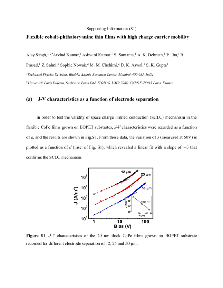
Supporting Information (S1) Flexible cobalt-phthalocyanine thin films with high charge carrier mobility Ajay Singh,1, 2*Arvind Kumar,1 Ashwini Kumar,1 S. Samanta,1 A. K. Debnath,1 P. Jha,1 R. Prasad,1 Z. Salmi,2 Sophie Nowak,2 M. M. Chehimi,2 D. K. Aswal,1 S. K. Gupta1 1 Technical Physics Division, Bhabha Atomic Research Center, Mumbai-400 085, India 2 Université Paris Diderot, Sorbonne Paris Cité, ITODYS, UMR 7086, CNRS F-75013 Paris, France (a) J-V characteristics as a function of electrode separation In order to test the validity of space charge limited conduction (SCLC) mechanism in the flexible CoPc films grown on BOPET substrates, J-V characteristics were recorded as a function of d, and the results are shown in Fig.S1. From these data, the variation of J (measured at 50V) is plotted as a function of d (inset of Fig. S1), which revealed a linear fit with a slope of ~-3 that confirms the SCLC mechanism. 12 m 25 m 5 4 10 50 m 3 10 2 J (A/m ) 2 J (A/m ) 10 2 10 5 10 3 10 20 d (m) 1 10 Slope ~ 3 4 10 1 10 Bias (V) 40 60 100 Figure S1: J-V characteristics of the 20 nm thick CoPc films grown on BOPET substrate recorded for different electrode separation of 12, 25 and 50 m. (b) Thickness dependent current density of CoPc films In order to investigate the dependence of J on the thickness of the CoPc films, films of different thickness i.e. 5, 10, 20, 40, 70 and 100 nm were grown on BOPET substrates under identical experimental conditions. Fig.S2 shows the thickness dependence of J (measured at 50 V) for CoPc films. It is evident that J attains a maximum value for the critical thickness of ~20 nm. For film thickness < 20 nm, low value of J is attributed to the incomplete coverage (mostly due to surface roughness ~ 6 nm). However for thickness >20 nm, the J gets suppressed due to enhanced molecular disorder (i.e. due to reduced effect of the interaction between substrate molecular chains and CoPc molecules). The higher molecular disorder in thicker film (70 nm) as compared to that of 20 nm thick film is evident from the XRD pattern shown in Fig. S2 (right). The thicker film (70 nm) shows a weak intensity of (200) peak along with a higher FWHM. Figure S2: Left: Variation of J (measured at 50 V) for CoPc films of various thicknesses grown on BOPET substrate. Right: XRD data of 20 and 70 nm thick CoPc films grown on BOPET substrate (c) Isotropic in-plane charge transport of CoPc films on BOPET In order investigate that if there is any in-plane anisotropy in the charge transport in 20 nm thick CoPc films grown on BOPET substrate, three pairs of gold electrodes were deposited in three different directions (at an angle of 45º) as shown in the inset of Fig. S3. From Fig. S3, it is evident that the J-V characteristics are almost identical for the three different electrode geometries used. This result therefore confirms that CoPc films on the BOPET substrate exhibits isotropic in-plane charge transport, which are in accordance with the pole figure measurements. Fig. S3: J-V characteristics of 20 nm thick CoPc films grown over BOPET substrate in three different electrode geometries shown in the inset. (d) Substrate dependent charge transport of CoPc films In order to investigate how the chemically non-interacting amorphous substrate influence the charge transport properties of CoPc films, 20 nm thick films were grown on glass and transparency sheet of the inkjet printer. The CoPc films prepared on glass substrate, as shown in Fig. S4, exhibit hysteretic J-V characteristics, which has been attributed to the presence structural defects and these studies are discussed in detail in our earlier publication.1 Figure S4: J-V characteristics for CoPc films grown on glass substrate. The films prepared on the transparency sheet of the inkjet printer shows non-hysteretic J-V characteristics, as shown in Fig. S5. However, the slope of J-V data at higher bias region is ~ 3.5, indicating the presence of exponential trap distribution in the films.2 Figure S5: J-V characteristics of CoPc films grown on smooth side of plastic transparency sheet of the inkjet printer References: 1. A. Singh, S. Samanta, A. Kumar, A. K. Debnath, D. K. Aswal, S. K. Gupta, J. V. Yakhmi, Y. Hayakawa, S. K. Deshpande, Org. Elec. 11, 1835 (2010). 2. R. D. Gould, Coord. Chem. Rev. 156, 237 (1996).

