Three-Dimensional Nanopatterning of Magnetic Materials
advertisement
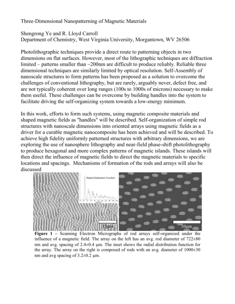
Three-Dimensional Nanopatterning of Magnetic Materials Shengrong Ye and R. Lloyd Carroll Department of Chemistry, West Virginia University, Morgantown, WV 26506 Photolithographic techniques provide a direct route to patterning objects in two dimensions on flat surfaces. However, most of the lithographic techniques are diffraction limited – patterns smaller than ~200nm are difficult to produce reliably. Reliable three dimensional techniques are similarly limited by optical resolution. Self-Assembly of nanoscale structures to form patterns has been proposed as a solution to overcome the challenges of conventional lithography, but are rarely, arguably never, defect free, and are not typically coherent over long ranges (100s to 1000s of microns) necessary to make them useful. These challenges can be overcome by building handles into the system to facilitate driving the self-organizing system towards a low-energy minimum. In this work, efforts to form such systems, using magnetic composite materials and shaped magnetic fields as "handles" will be described. Self-organization of simple rod structures with nanoscale dimensions into oriented arrays using magnetic fields as a driver for a curable magnetic nanocomposite has been achieved and will be described. To achieve high fidelity uniformly patterned structures with arbitrary dimensions, we are exploring the use of nanosphere lithography and near-field phase-shift photolithography to produce hexagonal and more complex patterns of magnetic islands. These islands will then direct the influence of magnetic fields to direct the magnetic materials to specific locations and spacings. Mechanisms of formation of the rods and arrays will also be discussed 15m 10m Figure 1 – Scanning Electron Micrographs of rod arrays self-organized under the influence of a magnetic field. The array on the left has an avg. rod diameter of 722±80 nm and avg. spacing of 2.4±0.4 m. The inset shows the radial distribution function for the array. The array on the right is composed of rods with an avg. diameter of 1000±30 nm and avg spacing of 3.2±0.2 m.
