Simple Filter Circuits
advertisement
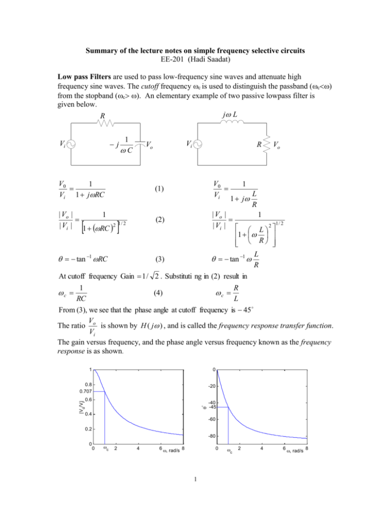
Summary of the lecture notes on simple frequency selective circuits EE-201 (Hadi Saadat) Low pass Filters are used to pass low-frequency sine waves and attenuate high frequency sine waves. The cutoff frequency c is used to distinguish the passband (c) from the stopband (c ). An elementary example of two passive lowpass filter is given below. j L R j Vi 1 C Vi Vo V0 1 Vi 1 jRC R V0 Vi (1) | Vo | 1 | Vi | 1 RC 2 Vo 1 1 j L R | Vo | 1 1/ 2 2 1/ 2 | Vi | L 1 R L q tan 1 RC (3) q tan 1 R At cutoff frequency Gain 1 / 2 . Substituti ng in (2) result in (2) 1 R (4) c RC L From (3), we see that the phase angle at cutoff frequency is 45 V The ratio o is shown by H ( j ) , and is called the frequency response transfer function. Vi The gain versus frequency, and the phase angle versus frequency known as the frequency response is as shown. c 1 0 0.8 0.707 -20 q° |Vo/Vi| 0.6 -40 -45 0.4 -60 0.2 -80 0 0 c 2 4 6 , rad/s 8 0 1 c 2 4 6 , rad/s 8 High pass Filters are used to stop low-frequency sine waves and pass the high frequency sine waves. The cutoff frequency c is used to distinguish the stopband (c) from the passband (c ). An elementary example of two passive highpass filter is given below. j 1 C R Vi R V0 RC Vi RC j1 Vo j L Vo Vi V0 Vi (5) | Vo | RC | Vi | RC 2 1 1 / 2 L R L j1 R L R | Vo | 1/ 2 2 | Vi | L 1 R 1 R q tan 1 (7) q tan 1 RC L At cut off frequency Gain 1 / 2 . Substituti ng in (6) result in (6) 1 R c RC L From (7), we see that the phase angle at cutoff frequency is 45 The gain versus frequency, and the phase angle versus frequency known as the frequency response is as shown. c 2 Bandpass Filters (a) The Parallel RLC Resonance IL IC j Ii 1 C j L IR R Vo Vo Ii 1 1 j ( C ) R L A circuit is in resonance when the voltage and current at the input terminals are in phase. 1 1 ) . At resonance Y is purely conductive and The circuit admittance is Y j ( C R L 1 1 C 0 , thus o . The circuit admittance is minimum or the circuit L LC impedance at resonance, given by Z ( o ) R , is maximum. Thus, the output voltage at resonance is maximum and is given by Vo ( o ) RI i 100 |Vo| = Ii/|Y|, V 80 V0(0) = RIi 70.71 60 40 20 0 0 1 100 o 2 300 200 400 , R/s 500 The frequencies 1 and 2 at which the output power drops to one half of its values at the resonant frequency are called the half-power frequencies. At these frequencies also known as cutoff frequencies or corner frequencies, the output voltage is | Vo ( c | 0.707 | Vo ( o ) | . This circuit which passes all the frequencies within a band of frequencies ( 1 2 ) is called a bandpass filter. This range of frequency is known as the circuit bandwidth. 2 1 The half-power frequencies are obtained from Ii 1 | Vo ( c ) | RI i 1 2 2 2 1 1 2 C L R Solving for we obtain 2 2 1 1 1 1 1 1 , and 2 1 2 RC LC 2 RC LC 2 RC 2 RC 3 1 , or the circuit bandwidth is RC 1 RC The cutoff frequencies can be written in terms of 0 and as follow: From the above, we obtain, 2 1 1 o 2 , and 2 o 2 2 2 2 2 This shows that o is the geometric mean of 1 and 2 , i.e., 2 2 o 1 2 Notice that is inversely proportional to R, i.e., smaller R results in a larger bandwidth. 1 The resonant frequency ( o ) is a function of L and C. Therefore, by adjusting L LC and C a desired resonant frequency is obtained, whereas by adjusting R, the bandwidth and the height of the response curve is adjusted. The sharpness of the resonance is measured quantitatively by the quality factor Q. This is defined as the ratio of the resonant frequency to the bandwidth. Q o 1 1 Substituting for and o the quality factor can be expressed as RC LC Q o RC At resonance IL and IC are given by Vo V IL j o jQI i and j o L R/Q R C R o L L I C j o CVo j Q Vo jQI i R I C jQI i Vo Ii I L jQI i As it can be seen at resonance depending on the Q factor, IL and IC can be many times the supply current (current amplification). 4 (b) The Series RLC Resonance 1 j C I j L Vi VC V L R Vo Vi I R j ( L 1 ) C A circuit is in resonance when the voltage and current at the input terminals are in phase. 1 ) . At resonance Z is purely resistive and The circuit impedance is Z R j ( L C 1 1 L 0 , thus o . The circuit impedance at resonance, given C LC by Z ( o ) R is minimum, and the current is maximum. Thus, the output voltage at resonance is maximum and is given by Vo ( o ) RI ( o ) 10 |Vo| = R|I( )|, V 8 V0(0) = RI(0) 7.071 6 4 2 0 0 1 100 o 2 200 300 400 , R/s 500 The frequencies 1 and 2 at which the output power drops to one half of its values at the resonant frequency are called the half-power frequencies. At these frequencies also known as cutoff frequencies or corner frequencies, the output voltage is | Vo ( c ) | 0.707 | Vo ( o ) | . This circuit which passes all the frequencies within a band of frequencies ( 1 2 ) is called a bandpass filter. This range of frequency is known as the circuit bandwidth. 2 1 The half-power frequencies are obtained from Vi 1 | Vo ( c ) | R Vi 1 2 2 2 1 2 R L C 5 Solving for we obtain 2 2 R 1 R 1 R R , and 2 1 2L LC 2L LC 2L 2L R From the above, we obtain, 2 1 , or the circuit bandwidth is L R L The cutoff frequencies can be written in terms of 0 and as follow: 1 o 2 , and 2 o 2 2 2 2 2 This shows that o is the geometric mean of 1 and 2 , i.e., 2 2 o 1 2 Notice that is proportional to R, i.e., larger R results in a larger bandwidth. The 1 resonant frequency ( o ) is a function of L and C. Therefore, by adjusting L and LC C a desired resonant frequency is obtained, whereas by adjusting R, the bandwidth and the height of the response curve is adjusted. The sharpness of the resonance is measured quantitatively by the quality factor Q. This is defined as the ratio of the resonant frequency to the bandwidth. Q o R 1 Substituting for and o the quality factor can be expressed as L LC o L 1 1 L R o RC R C At resonance VL and VC are given by VL j o LI ( 0 ) jQVi 1 VC j I ( 0 ) jQVi oC Q V L jQVi I Vi VC jQVi As it can be seen at resonance depending on the Q factor, VL and VC can be many times the supply voltage (voltage amplification). For a circuit with a very high quality factor Q, the corner frequencies may be approximated to 1 o , and 1 o 2 2 6 Bandreject Filter A bandreject filter is designed to stop all frequencies within a band of frequencies ( 1 2 ). In the series RLC circuit consider the output across the series combination L and C. R I V j L 1 R j ( L ) Vo C V o Vi 1 1 Vi j R j ( L ) C C The voltage gain magnitude is 1 L | Vo | C 2 1/ 2 | Vi | 1 2 R L C At 0 , the inductor behaves like a short circuit, and the capacitor behaves like an open circuit, I 0 and Vo Vi , and the voltage gain is unity. At , the inductor behaves like an open circuit and the capacitor behaves like a short circuit, I 0 and again Vo Vi , and the voltage gain is unity. At resonance Z is purely resistive and 1 1 L 0 , thus o . Since the numerator of the voltage gain is zero, the C LC gain drops to zero at o . 1 |Vo| = ( L-1/( C)|I|, V 0.8 .7071 0.6 0.4 0.2 0 0 1 100 o 2 200 300 400 , R/s 500 The cutoff frequencies, the bandwidth, and the quality factor are the same as the series R , 1 o 2 , and 2 o 2 L 2 2 2 2 2 RLC bandpass filter, 7 2 8
