Supplemental Material Enhanced charge−carrier injection caused
advertisement
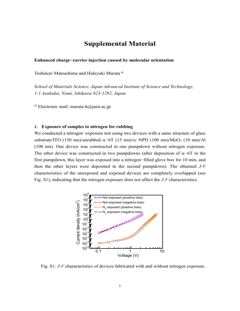
Supplemental Material Enhanced charge−carrier injection caused by molecular orientation Toshinori Matsushima and Hideyuki Murata a) School of Materials Science, Japan Advanced Institute of Science and Technology, 1-1 Asahidai, Nomi, Ishikawa 923-1292, Japan a) Electronic mail: murata-h@jaist.ac.jp 1. Exposure of samples to nitrogen for rubbing We conducted a nitrogen−exposure test using two devices with a same structure of glass substrate/ITO (150 nm)/unrubbed −6T (15 nm)/−NPD (100 nm)/MoO3 (10 nm)/Al (100 nm). One device was constructed in one pumpdown without nitrogen exposure. The other device was constructed in two pumpdowns (after deposition of −6T in the first pumpdown, this layer was exposed into a nitrogen−filled glove box for 10 min, and then the other layers were deposited in the second pumpdown). The obtained J-V characteristics of the unexposed and exposed devices are completely overlapped (see Fig. S1), indicating that the nitrogen exposure does not affect the J-V characteristics. 2 Current density (mA/cm ) 5 10 4 10 3 10 2 10 1 10 0 10 -1 10 -2 10 -3 10 -4 10 -5 10 -6 10 Not exposed (positive bias) Not exposed (negative bias) N2 exposed (positive bias) N2 exposed (negative bias) 0.1 1 Voltage (V) 10 Fig. S1. J-V characteristics of devices fabricated with and without nitrogen exposure. 1 2. Origin of absorption peaks of −6T It is well known that aggregation of molecules with their long axes parallel to each other (H-aggregate) induces a shift of an absorption peak to blue (a shorter wavelength) (Phys. Rev. B 54, 2198 (1996).). Egelhaaf et al. reported that a thin −6T film had a sharp blue−shifted absorption peak originating from aggregates of standing −6T molecules on a silica substrate and that an increase in −6T thickness reduced an intensity of the sharp absorption and increased its vibronic side bands due to reduced molecular order for the thick films (Synth. Met. 61, 143 (1993)). The spectral shapes of our unrubbed and rubbed −6T films (Figs. 3(a) and 3(b)) are respectively similar to those of the thin and thick −6T films reported by Egelhaaf et al. Alternatively, Oelkrug et al. explained that the sharp blue−shifted absorption peak of an −6T film with standing molecules compared with lying molecules came from anisotropy of molecules (optics effect) (Thin Solid Films. 284−285, 267 (1996).). The spectral shape of our unrubbed −6T film is similar to that of the −6T film reported by Oelkrug et al. as well. In our −6T films, the ≈360 nm sharp absorption peak decrease and the 400−600 nm absorption peaks relatively increase in absorbance by the rubbing (Figs. 3(a) and 3(b)). Moreover, no peak shift is observed after the rubbing. Since it is difficult to explain these rubbing−induced spectral changes using the optics effect, a change in aggregation condition caused by the rubbing affects the spectral shapes more strongly than the optics effect. Thus, we assume that the strong absorption peak at ≈360 nm and the weak absorption peaks ranging from 400 to 600 nm arise from aggregated and unaggregated molecules, respectively. 2 3. Polarized absorption spectra of 5 nm −6T thin film The polarized absorption spectra of a 5 nm −6T thin film on a fused silica substrate were measured under normal and oblique light incidence using an UV−visible absorption spectrometer (V670, JASCO). There is no absorption dichroism under the normal incidence [Fig. S2(a)], meaning that both aggregated and unaggregated molecules are random in the film plane. With the oblique incidence, the p−polarized spectrum is much larger in absorbance than the s−polarized spectrum in the shorter−wavelength region and the longer−wavelength absorption is unpolarized [Fig. S2(b)]. Thus, it is inferred that unaggregated molecules are also random in the thickness direction, but the standing orientation of aggregated molecules is dominant for the as−deposited 5 nm −6T thin film. These results agree with those obtained from the as−deposited 15 nm −6T film [Figs. 2(a) and 2(b)] and indicate that aggregated−6T molecules of the initial few layers are standing on the substrate surface as well. Fig. S2. Polarized absorption spectra of 5 nm −6T film on fused silica substrate with (a) normal and (b) oblique light incidence. 3 4. X-ray diffraction (XRD) spectra We measured the XRD spectra of the 15 nm unrubbed and rubbed −6T films on fused silica substrates (Fig. S3) and on ITO−coated glass substrates (Fig. S4) using a 2/ technique (CuK: =1.54 Å) (M18XHF, MAC Science). We also measured the XRD spectra of 5, 10, and 15 nm pentacene thin films on fused silica substrates and −6T powder for comparison (Fig. S5). The vacuum deposition rate of pentacene was set at 0.01 nm/s. The −6T powder (Aldrich) was purified twice using temperature gradient vacuum sublimation prior to the XRD measurement. The unrubbed and rubbed−6T films exhibit no clear XRD peak and the spectral shapes of the films agree well with those of the bare substrates. On the other hand, we can obtain clear XRD peaks from the pentacene thin films and the −6T powder. The lattice spacing can be calculated to be 15.3 Å from the pentacene peaks using a conventional Bragg equation, which corresponds to a thin film phase (Synth. Met. 104, 175 (1999)). Therefore, no peak observation from the −6T films indicates rather little crystallization. Fig. S3. XRD spectra of unrubbed and rubbed −6T films on fused silica substrates. 4 Fig. S4. XRD spectra of unrubbed and rubbed −6T films on 150 nm ITO surfaces. Fig. S5. XRD spectra of 5, 10, and 15 nm pentacene films and −6T powder. 5 5. AFM images of as−deposited and rubbed −6T films Fig. S6. All AFM images of as−deposited and rubbed −6T films. 6 6. Polarized absorption spectra of 10 nm −NPD on 15 times rubbed −6T Fig. S7. Polarized absorption spectra of 10 nm −NPD film on 15 times rubbed −6T surface measured with (a) normal and (b) oblique light incidence. 7

