CMOS Device Modelling for Circuit Design

57
Appendix A
CMOS Device Modeling for Circuit
Design
Before a circuit is designed, to be integrated by CMOS VLSI technology, a model must be adopted which will describe behavior of all components successfully.
A model means a set of mathematical formulas, circuit representations, tables, reference standards etc.
A.1. Simple MOS large signal model
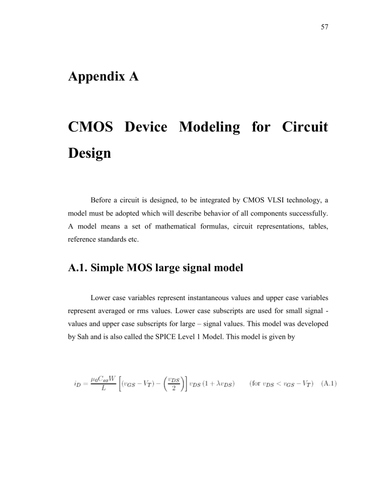
Lower case variables represent instantaneous values and upper case variables represent averaged or rms values. Lower case subscripts are used for small signal - values and upper case subscripts for large – signal values. This model was developed by Sah and is also called the SPICE Level 1 Model. This model is given by
58
59
60
A.2. Simple MOS Small – Signal Model
61
62
Appendix B
The Cadence IC 445 set of tools
The IC 4.4.5 set of tools is a complete front-end to back-end design suite for integrated circuit design. This chapter gives a summary of the different design tools available to an analog circuit designer.
B.1 Design Entry
For analog design, the Composer Schematic Editor tool is used. This allows easy entry of the schematic. The editor employs several useful options to make design entry efficient. Some of these include gravity, object sensitive dialogs and pop-up menus. It also includes a method for checking the validity of the design. The schematic entry environment extracts a netlist called the CDL.
B.2 Simulation Environment
The analog artist simulation environment is used to simulate the design. This is a front-end to the actual simulator. It allows one to choose the simulator and set the
54 options appropriate for the simulator through easy to use menus. Analog artist also includes extensive post-processing facilities for analyzing the results of the circuit
63 simulation. Analog artist contains support for cdsSPICE, spectreS, HSPICE and other simulators. cdsSPICE and spectreS are Cadence's simulators based on SPICE but with some extensions. It supports all standard SPICE models. Specifically, BSIM3v3 models were used for the simulation of the circuits.
B.3 Design Synthesis and Layout
The device level editor (DLE) is used to generate the layout from the schematic. This places all the devices in a layout window approximately in accordance with their placement in the schematic. This also has facility for showing the devices and nets that need to be connected. This allows one to do a layout that corresponds exactly to the schematic. The Virtuoso layout editor is used for defining the interconnects and other structures in the layout.
B.4 Design Verification
Once the layout is made, it has to be verified to be correct. For this, one does a design rule check (DRC) using the Diva verification tool. After the design rule check has been passed, a netlist has to be extracted from the layout. This netlist is then compared with the schematic netlist using the “Layout vs. Schematic” option in Diva.
Diva also contains options for extraction of parasitic resistance and capacitance. This information can be back annotated into the circuit and the simulation repeated to verify that the circuit does indeed work with the parasitics.
Appendix C
Acronyms
ADC
Analog to Digital Converter
BiCMOS
Bipolar Complementary Metal Oxide Semiconductor
BJT
CAD
Bipolar Junction Transistor
Computer Aided Design
CMOS
Complementary Metal Oxide Semiconductor
DAC
Digital to Analog Converter
IC
MOS
Integrated Circuit
Metal Oxide Semiconductor
MOSFET
Metal Oxide Semiconductor Field Effect Transistor
VLSI
Very Large Scale Integration
64
65
Bibliography
[1] S. M. Sze, Physics of Semiconductor Devices, John Wiley & Sons Inc., 1981
( A.1 )
[2] P. Allen and Holberg, CMOS Analog Integrated Circuits, Holt, Rinehart and
Winston, 1987 ( A.1 , A.2 )
[3] Laker, K. R., and Sansen, W. M. C., Design of Analog Integrated Circuits and
Systems, McGraw-Hill, Inc., 1994. ( A.1 , A.2 )
[4] Gray, P. R., & Meyer, Analysis and Design of Analog Integrated Circuits, Third
Ed., John Wiley & Sons Inc., 1995. ( A.1 , A.2 )
[5] R.R. Harrison, P. Hasler, and B.A. Minch, “Floating-Gate CMOS Analog
Memory Cell Array”,
Proceedings of the IEEE International Symposium on
Circuits and Systems, Monterey, Vol. 2, pp . 204-207, 1998.
[6] B. Wang, J. R. Hellums, G. C. Sodini, “MOSFET thermal noise modelling for analog integrated circuits”, IEEE JSSC , Vol. 29, No. 7, pp. 833-835, July
1994. (A.1 )
66
[7] A. Simoni, A. Sartori, M. Gottardi, and A. Zorat, “A digital vision sensor”,
Sensors and Actuators A (Physical) , vol. A47, no. 1-3, pp. 439-443, March-April
1995. (2.3.2)
[8] A. Simoni, G. Torelli, F. Maloberti, A. Sartori, S.E. Plevridis, and A.N. Birbas,
“A single-chip optical sensor with analog memory for motion detection”, IEEE J.
Solid State Circuits , vol. 30, no. 7, pp. 800-806, July 1995. ( 2.3.2 )
[9] R. Carmona, S. Espejo, R. Domínguez-Castro, A. Rodríguez-Vázquez, T. Roska,
T. Kozek and L. O. Chua, “A 0.5µm CMOS CNN Analog Random Access
Memory Chip for Massive Image Processing”,
Proc. of the Fifth IEEE Int.
Workshop on Cellular Neural Networks and their Applications , pp. 243-248,
London, UK, April 1998.
[10] R. Carmona, S. Espejo, R. Domínguez-Castro, A. Rodríguez-Vázquez, T. Roska,
T. Kozek and L. O. Chua, “A 0.5µm CMOS Random Access Analog Memory
Chip for TeraOPS Speed Multimedia Video Processing”,
IEEE Transactions on
Multimedia.
(Accepted for publication in 1999).
[11] Philipp Häfliger and Christoph Rasche, “Floating gate analog memory for parameter and variable storage in a learning silicon neuron”,
IEEE International
Symposium on Circuits and Systems , 1999.
[12] G. Cauwenberghs, “Analog VLSI Long-Term Dynamic Storage”, Proceedings of
the International Symposium on Circuits and Systems, Atlanta, GA, 1996.
67
[13] G. Cauwenberghs, and A. Yariv, “Fault-Tolerant Dynamic Multi-Level Storage
in Analog VLSI”, IEEE Transactions on Circuits and Systems II, vol. 41 (12), pp 827-829, 1994.
[14] Y. Horio, and S. Nakamura, “Analog Memories for VLSI Neurocomputing”,
Artificial Neural Networks: Paradigms, Applications, and Hardware
Implementations , C. Lau and E. Sanchez-Sinencio, Eds., IEEE Press, pp 344-
363, 1992.
[15] Y. Nitta, J. Ohta, S. Tai, and K. Kyuma, “Optical learning neurochip with internal analog memory”,
Applied Optics , vol. 32, no. 8, pp. 1264-1274, Mar.
1993.
[16] R.C. Meitzler, A.G. Andreou, K. Strohbehn, and R.E. Jenkins, “A sampled-data motion chip”,
Proc. Midwest Symposium on Circuits and Systems , vol. 1, pp.
288-291, 1993.
[17] I. Masaki, L.R. Carley, S. Decker, B.K.P Horn, H.S. Lee, D.A. Martin, C.G.
Sodini, and J.L. Wyatt, “New architecture paradigms for analog VLSI chips”,
Vision Chips, Implementing Vision Algorithms Using Analog VLSI Circuits , C.
Koch and H. Li, Eds., pp. 353-375. IEEE Press, 1994.
[18] E. Franchi, M. Tartani, R. Guerrieri, and G. Baccarani, “Random access analog memory for early vision”,
IEEE J. Solid State Circuits , vol. 27, no. 7, pp. 1105-
1109, July 1992.
68
[19] Hastings, Alan, The Art of Analog Layout, Prentice-Hall, Inc., 1999.
[20] Montoro, C. G., Schneider, M. C., Cunha, A. I. A., “A current-based MOSFET model for integrated circuit design”, Low-Voltage/Low-Power Integrated
Circuits and Systems , Sanchez-Sinencio, E., Andreou, A. G., ed., IEEE Press,
1999.


