Word version - University of California, Berkeley
advertisement
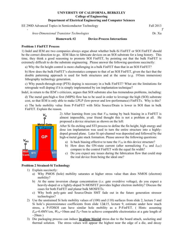
UNIVERSITY OF CALIFORNIA, BERKELEY College of Engineering Department of Electrical Engineering and Computer Sciences EE 290D Advanced Topics in Semiconductor Technology hree-Dimensional Transistor Technologies Homework #2 Fall 2013 T Dr. Xu Device-Process Interactions Problem 1 FinFET Process 1) Indel and IEM are two companies always argue about whether bulk-Si FinFET or SOI FinFET should be the correct direction to go. IEM likes to fabricate devices on an SOI substrate for a long history. This time, they think a good reasoning to promote SOI FinFET, by pointing out that the bulk FinFET is extremely difficult to do the substrate engineering. Please answer the following questions succinctly: a) Why the fin height control is more challenging in a bulk FinFET than that in an SOI FinFET? b) How does the bulk FinFET’s electrostatics compare to that of an SOI FinFET, given the fact that the double patterning approach is used for both structures and at the same (e.g. 193nm immersion) lithography technology generation. c) Why punch-through-stop (PTS) doping is necessary in a bulk FinFET? What are the limitations for retrograde well doping if it is simply implemented by ion implantation technique? Indel, in return to the IEM’s criticizes, argues that SOI substrate also has tremendous problems, including: d) The metal gate/high-κ first (MIPS) flow has to be used in order to leverage the high (SOI) substrate cost, so that IEM is only able to make LPLP (low-power and low-performance) FinFETs. Why is this? e) The hole mobility value from P-FinFET with SiGe Source/Drain is lower in SOI than in bulk FinFET. Explain the reason. 2) After learning from you that VTH tuning by back biasing in a FinFET is VG almost impossible, your friend thought this is not a problem at all. He proposed a device structure as shown on the left: Metal Gate After Si fin etching and STI process to define the fin height, high energy and Si channel dose ion implantation was used to turn the entire structure into a highlydoped ground plane. Later Si epi-channel was deposited and followed by the high-κ/metal gate stack formation. Please answer the following questions: GP VBG a) Is back biasing effective to tune the VTH in this device structure? b) How does the ON-state current (after normalizing VTH and IOFF) compare to the control FinFET with the equal fin width? Well STI STI c) Do you expect any issues during the fabrication flow that could stop Cont. the real device from being the ideal one? Problem 2 Strained-Si Technology 1) Explain succinctly: a) Why PMOS (hole) mobility saturates at higher stress value than does NMOS (electron) mobility? b) At the same inversion charge concentration (i.e. gate overdrive voltage), do you expect a heavily-doped or a lightly-doped N-MOSFET provides higher electron mobility? Discuss the cases for both FinFET and planar bulk MOSFETs. c) Why both poly-gate and Source/Drain SMT fade out in the future generation stressor technologies? 2) Use the unstrained Si hole mobility values of (100) and (110) surfaces from slide 2, lecture 5 and Si hole’s piezoresistance coefficients from slide 12&15, lecture 9, estimate under how much stress, a P-FDSOI can have similar hole mobility as a P-FinFET. ( Hints: assuming Eeff=0.4MV/cm, WFin=10nm and TSi=5nm to achieve comparable electrostatics at a gate length of ~20nm ) 3) Die packaging process can induce in-plane biaxial stress due to the board attach, socketing and thermal solution. The stress values will appear the highest near the edge of a die, and decay towards the center (i.e. the devices around the die edge will be mostly affected). Based on the PMOS current % change (to nominal devices) shown below, can you tell whether the stress is compressive or tensile? Problem 3 Performance Variability 1) Answer the following questions succinctly regarding Random Dopants Fluctuations (RDF): a) Do you expect RDF will be more harmful to low-power (LP) or high-performance (HP) devices? Why? b) Do you expect the RDF-caused MOSFET performance variability will be larger in ION or IEFF (by evaluating the % change)? Why? c) Regarding the back biasing knobs used for UTBB FD-SOI MOSFET’s performance tuning, do you expect VTH variability will be larger in devices w/ RBB or w/FBB? Why? (Hints: assuming an identical VTH for all back biasing conditions) d) Why Takeuchi plots can isolate the impacts of MOSFET’s oxide thickness and channel doping on evaluating the RDF “magnitude”, as compared to Pelgrom plot?


