Crystal Defects – Enhancing Silicon Semiconductor Properties by
advertisement
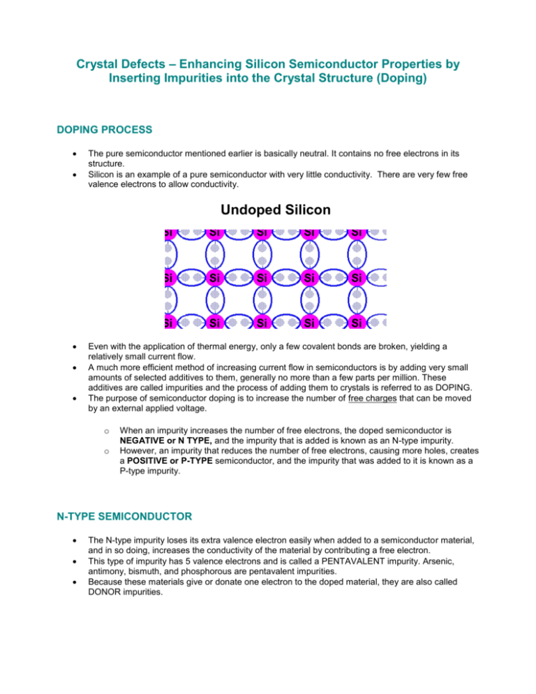
Crystal Defects – Enhancing Silicon Semiconductor Properties by Inserting Impurities into the Crystal Structure (Doping) DOPING PROCESS The pure semiconductor mentioned earlier is basically neutral. It contains no free electrons in its structure. Silicon is an example of a pure semiconductor with very little conductivity. There are very few free valence electrons to allow conductivity. Undoped Silicon Even with the application of thermal energy, only a few covalent bonds are broken, yielding a relatively small current flow. A much more efficient method of increasing current flow in semiconductors is by adding very small amounts of selected additives to them, generally no more than a few parts per million. These additives are called impurities and the process of adding them to crystals is referred to as DOPING. The purpose of semiconductor doping is to increase the number of free charges that can be moved by an external applied voltage. o o When an impurity increases the number of free electrons, the doped semiconductor is NEGATIVE or N TYPE, and the impurity that is added is known as an N-type impurity. However, an impurity that reduces the number of free electrons, causing more holes, creates a POSITIVE or P-TYPE semiconductor, and the impurity that was added to it is known as a P-type impurity. N-TYPE SEMICONDUCTOR The N-type impurity loses its extra valence electron easily when added to a semiconductor material, and in so doing, increases the conductivity of the material by contributing a free electron. This type of impurity has 5 valence electrons and is called a PENTAVALENT impurity. Arsenic, antimony, bismuth, and phosphorous are pentavalent impurities. Because these materials give or donate one electron to the doped material, they are also called DONOR impurities. ARSENIC DOPING IN SILICON ( n - DOPING ) P-TYPE SEMICONDUCTOR The second type of impurity, when added to a semiconductor material, tends to compensate for its deficiency of 1 valence electron by acquiring an electron from its neighbor. Impurities of this type have only 3 valence electrons and are called TRIVALENT impurities. Aluminum, indium, gallium, and boron are trivalent impurities. Because these materials accept 1 electron from the doped material, they are also called ACCEPTOR impurities. GALLIUM DOPING IN SILICON ( p - DOPING ) Doping is the process by which engineers change an insulating material into a semiconductor. The basic process inserts a small 'population ' of a foreign element into the crystal lattice of the insulator. While n-doping adds extra electrons, p-doping results in the generation of holes. A hole is the absence of an electron, which is treated as a positive charge carrier. If we had implanted Gallium (Ga) in the Silicon, one bond would be missing because Ga only has 3 valence electrons. Thus, a hole has been created, an entity which can propagate through the crystal by grabbing a nearby valence electron and creating a new hole. In this way the hole propagates and is considered the flow of positive charge.
