Dip Pen Nanolithography (DPN): Nanoscale Patterning Method
advertisement
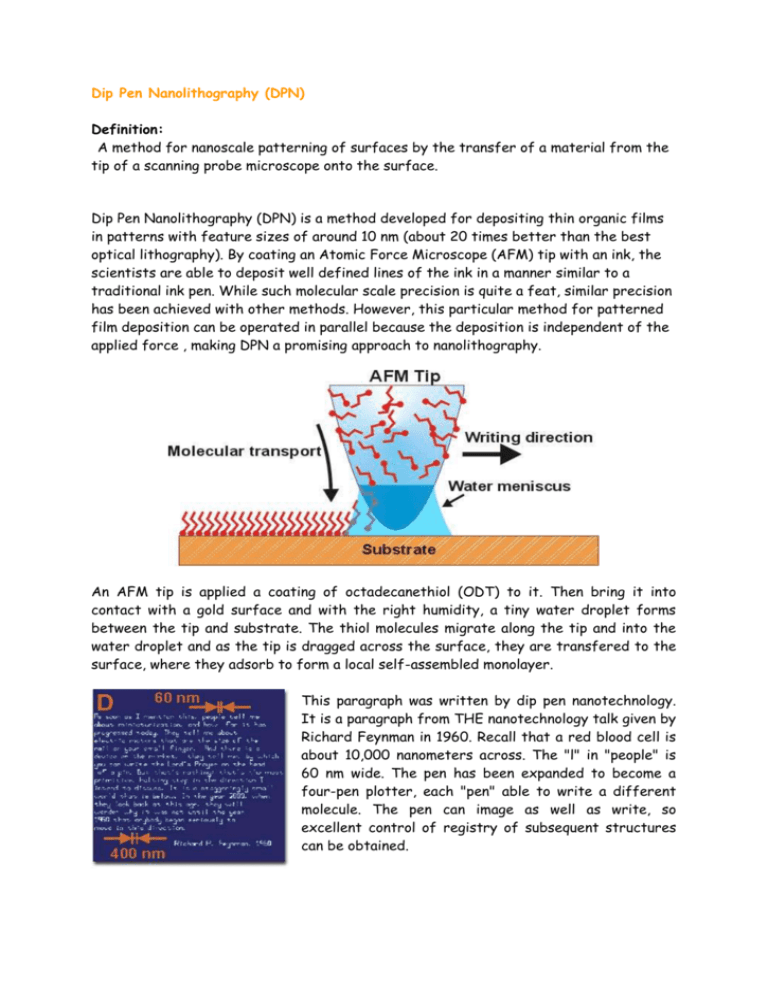
Dip Pen Nanolithography (DPN) Definition: A method for nanoscale patterning of surfaces by the transfer of a material from the tip of a scanning probe microscope onto the surface. Dip Pen Nanolithography (DPN) is a method developed for depositing thin organic films in patterns with feature sizes of around 10 nm (about 20 times better than the best optical lithography). By coating an Atomic Force Microscope (AFM) tip with an ink, the scientists are able to deposit well defined lines of the ink in a manner similar to a traditional ink pen. While such molecular scale precision is quite a feat, similar precision has been achieved with other methods. However, this particular method for patterned film deposition can be operated in parallel because the deposition is independent of the applied force , making DPN a promising approach to nanolithography. An AFM tip is applied a coating of octadecanethiol (ODT) to it. Then bring it into contact with a gold surface and with the right humidity, a tiny water droplet forms between the tip and substrate. The thiol molecules migrate along the tip and into the water droplet and as the tip is dragged across the surface, they are transfered to the surface, where they adsorb to form a local self-assembled monolayer. This paragraph was written by dip pen nanotechnology. It is a paragraph from THE nanotechnology talk given by Richard Feynman in 1960. Recall that a red blood cell is about 10,000 nanometers across. The "l" in "people" is 60 nm wide. The pen has been expanded to become a four-pen plotter, each "pen" able to write a different molecule. The pen can image as well as write, so excellent control of registry of subsequent structures can be obtained. The plan here is to use the dip pen to pattern a substrate and develop an array of binding sites on a substrate surface. The pen can write to differently functionalize each site, enabling a combinatorial analysis of biological or catalytic reactions. This surface was "painted" with the dip pen nanoprobe. This is a monolayer of ODT. The registry and order of the layer is clearly evident, and is confirmed by the remarkably sharp TEM diffraction pattern inset.
