Assignment
advertisement
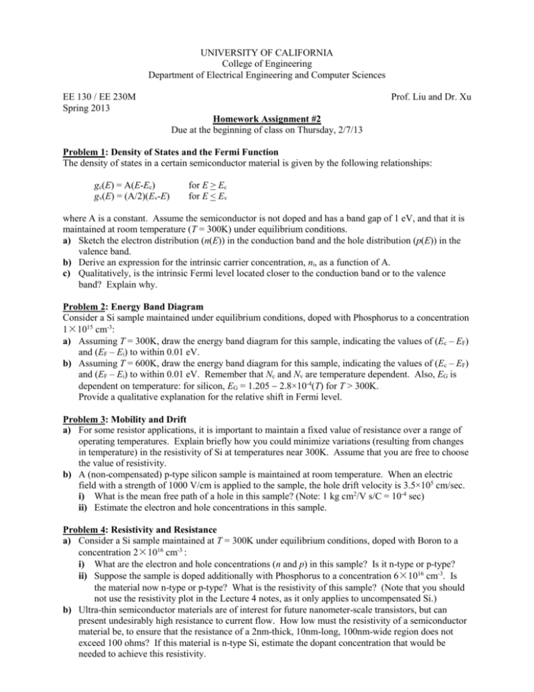
UNIVERSITY OF CALIFORNIA College of Engineering Department of Electrical Engineering and Computer Sciences EE 130 / EE 230M Spring 2013 Prof. Liu and Dr. Xu Homework Assignment #2 Due at the beginning of class on Thursday, 2/7/13 Problem 1: Density of States and the Fermi Function The density of states in a certain semiconductor material is given by the following relationships: gc(E) = A(E-Ec) gv(E) = (A/2)(Ev-E) for E > Ec for E < Ev where A is a constant. Assume the semiconductor is not doped and has a band gap of 1 eV, and that it is maintained at room temperature (T = 300K) under equilibrium conditions. a) Sketch the electron distribution (n(E)) in the conduction band and the hole distribution (p(E)) in the valence band. b) Derive an expression for the intrinsic carrier concentration, ni, as a function of A. c) Qualitatively, is the intrinsic Fermi level located closer to the conduction band or to the valence band? Explain why. Problem 2: Energy Band Diagram Consider a Si sample maintained under equilibrium conditions, doped with Phosphorus to a concentration 1×1015 cm-3: a) Assuming T = 300K, draw the energy band diagram for this sample, indicating the values of (Ec – EF) and (EF – Ei) to within 0.01 eV. b) Assuming T = 600K, draw the energy band diagram for this sample, indicating the values of (Ec – EF) and (EF – Ei) to within 0.01 eV. Remember that Nc and Nv are temperature dependent. Also, EG is dependent on temperature: for silicon, EG = 1.205 2.8×10⁻⁴(T) for T > 300K. Provide a qualitative explanation for the relative shift in Fermi level. Problem 3: Mobility and Drift a) For some resistor applications, it is important to maintain a fixed value of resistance over a range of operating temperatures. Explain briefly how you could minimize variations (resulting from changes in temperature) in the resistivity of Si at temperatures near 300K. Assume that you are free to choose the value of resistivity. b) A (non-compensated) p-type silicon sample is maintained at room temperature. When an electric field with a strength of 1000 V/cm is applied to the sample, the hole drift velocity is 3.5×105 cm/sec. i) What is the mean free path of a hole in this sample? (Note: 1 kg cm2/V s/C = 10-4 sec) ii) Estimate the electron and hole concentrations in this sample. Problem 4: Resistivity and Resistance a) Consider a Si sample maintained at T = 300K under equilibrium conditions, doped with Boron to a concentration 2×1016 cm-3 : i) What are the electron and hole concentrations (n and p) in this sample? Is it n-type or p-type? ii) Suppose the sample is doped additionally with Phosphorus to a concentration 6×1016 cm-3. Is the material now n-type or p-type? What is the resistivity of this sample? (Note that you should not use the resistivity plot in the Lecture 4 notes, as it only applies to uncompensated Si.) b) Ultra-thin semiconductor materials are of interest for future nanometer-scale transistors, but can present undesirably high resistance to current flow. How low must the resistivity of a semiconductor material be, to ensure that the resistance of a 2nm-thick, 10nm-long, 100nm-wide region does not exceed 100 ohms? If this material is n-type Si, estimate the dopant concentration that would be needed to achieve this resistivity.
