BOSS_manual
advertisement
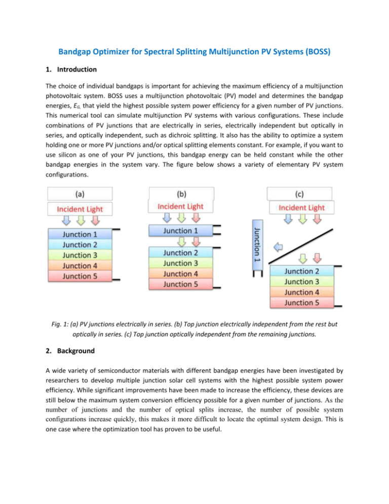
Bandgap Optimizer for Spectral Splitting Multijunction PV Systems (BOSS) 1. Introduction The choice of individual bandgaps is important for achieving the maximum efficiency of a multijunction photovoltaic system. BOSS uses a multijunction photovoltaic (PV) model and determines the bandgap energies, EG, that yield the highest possible system power efficiency for a given number of PV junctions. This numerical tool can simulate multijunction PV systems with various configurations. These include combinations of PV junctions that are electrically in series, electrically independent but optically in series, and optically independent, such as dichroic splitting. It also has the ability to optimize a system holding one or more PV junctions and/or optical splitting elements constant. For example, if you want to use silicon as one of your PV junctions, this bandgap energy can be held constant while the other bandgap energies in the system vary. The figure below shows a variety of elementary PV system configurations. Fig. 1: (a) PV junctions electrically in series. (b) Top junction electrically independent from the rest but optically in series. (c) Top junction optically independent from the remaining junctions. 2. Background A wide variety of semiconductor materials with different bandgap energies have been investigated by researchers to develop multiple junction solar cell systems with the highest possible system power efficiency. While significant improvements have been made to increase the efficiency, these devices are still below the maximum system conversion efficiency possible for a given number of junctions. As the number of junctions and the number of optical splits increase, the number of possible system configurations increase quickly, this makes it more difficult to locate the optimal system design. This is one case where the optimization tool has proven to be useful. BOSS simulates the terminal current-voltage characteristics of each individual PV junction. These results are then used to determine the overall system power efficiency. The short-circuit current density (𝐽𝑠𝑐 ) is found by assuming a specific collection efficiency above the bandgap energy of each junction. This allows (𝐽𝑠𝑐 ) to be equal to the collected light current (𝐽𝐿 ) as shown below EG ,i 1 J SC ,i J L ,i q E dE EG ,i Where i is the junction number, q is the electron charge, and E is the photon flux density per unit energy of the incident light spectrum. The current-voltage characteristic are simulated using the ideal diode equation with series resistance as J i J SC ,i J 0,i e q Vi RS ,i Ji ni kT 1 Where V is the voltage, 𝑅𝑆 is the series resistance, n is the ideality factor, k is the boltzmann constant, and T is the temperature. A bisection method is used to find the maximum output power of each of the PV junctions. The current at maximum power point is given by J SC ,i J 0,i J MP ,1 N n kT ln R J i S ,i MP ,1 N J i 1 0, i N ni kT R S ,i J J J j 1 SC , i 0, i MP ,1 N N J MP ,1 N Where N is the number of junctions. Each individual junction voltage is give as J J 0,i J MP,1 N VMP,i nkT ln SC ,i J 0,i RS ,i J MP,1 N Therefore, the total voltage in an ith PV device for a series connected stack is just the sum of these voltages N VMP ,1 N VMP ,i i 1 Finally we can determine the total instantaneous maximum output power of the system as Pout N J i 1 VMP ,i MP , i The tool has built-in models for the reverse saturation current density (𝐽0 ). The first model is the Shockley-Queisser detailed balance radiative limit and the second is a simple empirical expression obtained from published “state-of-the-art” solar cells performance characteristics. The ShockleyQueisser limit used to estimate the saturation current density is as follows J 0,i 2 kT q hc 3 2 3 E e G ,i kT EG ,i 2 EG ,i 2 kT 2 kT Where h is plank’s constant and c is the speed of light. The “stat-of-the-art” model used to estimate the saturation current density is J 0,i 1.14 109 exp(40.5EG,i ) In BOSS, the PV model for each junction is simulated inside of an algorithm for determining the optimal bandgap energies. This algorithm uses a multidimensional unconstrained nonlinear minimization method (Nelder-Mead). When there are optical splits involved in a system, some of the incident light is reflected and some are transmitted. The figure below shows the general principle of how light is reflected and transmitted in an optically split system. Fig. 2: Diagram showing how incident light is reflected and transmitted in an optically split system. 3. Using the tool Like any other software tool, there are input parameters required in order to get your desired output. Fig. 3 shows the device input parameters and Fig. 4 shows the global input parameters. As can be seen at the bottom of the interface screen there is an example tab that has various PV configuration examples to help first time users get acquainted with the tool. Fig. 3: Interface showing device input parameters. Fig. 4: Interface showing global input parameters. A description of each of the input parameters (both device and global) and their character types are given in the table below Table 1: Tool input parameters and descriptions Device parameters Type Default Units Number of splits Integer 0 Number of junctions Integer 1 Electrically in series String yes Initial band gap energy Integer 1 eV Series resistance Collection efficiency Initial optical split cut-off Optical split transition width Integer 0 𝛀/𝑐𝑚2 Integer 1 ratio Integer -100 eV Integer 0 μm Reflectivity Integer 1 ratio Transmission loss integer 0 ratio Global parameters Geometric concentration Operating temperature Type Default Units Integer 300 suns Integer 300 kelvin Solar spectrum file String am1.5dc Junction Jo model String s-q Junction Jo derate Number of iterations Closest Eg spacing Integer 1 Integer 10 Integer 0.03 ratio eV Description The number of optical splits in the system – each optical split adds a PV junction stack to the system The number of PV junctions contained in each stack Choose whether a junction is electrically in series with the junction above it Bandgap energy used in the first iteration of the optimization - negating bandgap will stop bandgap from changing during optimization. Series resistance component of this junction Current collection efficiency ratio The initial photon energy of the optical transition of this split The optical transition width in wavelength of this split The efficiency ratio of light transmitted by this split to a stack , with photon energies above the optical transition width range of the split The efficiency ratio of light transmitted by this split to the next split, with photon energies below the optical transition width range. If there is not another split below this in the system, the light will be directed to last stack Description The geometric concentration of the system The operating temperature of each PV junction Input solar spectrum file which contains am1.5dc, am1.5g, am0, and blackbody Reverse saturation current density model used to determine the JO of each junction based on the EG Coefficient used to adjust the the JO model Number of iterations attempted to get the optimum bandgaps Closest allowable bandgap energy spacing 3.1 Instructions for tool When entering the initial bandgap energies for a PV system, it is important to ensure that they are in descending order from the first junction to the last. The bandgap energies for each junction should be at least 0.1 eV apart from each other. To keep the bandgap energy of a PV junction from optimizing (holding it constant); simply add a negative sign “-” to the bandgap value. The “electrically in series” tab in each junction gives the option for that junction to be electrically in series or independent to the junction above it. When a junction is electrically independent from another it creates sub-stacks with in a stack. To have a split in a configuration simply click on the “number of splits’’ tab and choose the number of splits. The number of stacks created by the tool will always be 1 more than the number of splits chosen. The “initial optical split cut-off” is selected based on the configuration of the system. For example, if the user wants the optical split to be below the junction with bandgap energy of 2 eV, then the “initial optical split cut-off” will be 2 eV. The “Junction Jo model” tab allows the user to choose a reverse saturation current density model. “s-q” is for The Shockley-Queisser limit and “sota” is for the “state of the art” model. The tool interface has examples of all possible configurations that the program can simulate. These examples together with the above instructions make it easy for the user to understand this tool. 4. Generated outputs (I) The tool generates the optimum band gap for each junction in the system along with the efficiency associated with that individual band gap as shown below Fig. 5: Efficiency of each individual band gap in a 5-junction PV system. (II) The tool generates other important solar cell parameters that are found in the output log of the results tab. These parameters are listed in the table below along with their description Table 2: Output parameters and descriptions Parameters Eg Jsc Voc Jmp Vmp FF FFi Jo Jo (D) Power (in) Power (out) Total Efficiency Optical split cut-off Description Optimum bandgap energy Short circuit current Open circuit voltage Current at max power point Voltage at max power point Fill factor which is the ratio of the maximum power of the system to the product of Voc and Jsc Intrinsic fill factor Reverse saturation current density Derating coefficient used to adjust the the Jo model Solar spectrum input power to the PV system Power generated by the PV system Efficiency of the PV system which is the ratio of the Power (in) to the Power (out) Optimized photon energy of the optical transition of a split (III) Plots of the solar spectrum as well as how the solar spectrum is absorbed by each junction are generated by this tool. The solar spectrum is absorbed by the junctions in a PV system based on the energy of the photons in the spectrum. Photons with energy less than the bandgap energy are not absorbed and passed on to the lower energy bandgaps. Examples of both plots are shown in Fig. 4 and Fig. 5. Fig. 6: Plot showing am1.5dc spectrum. Fig. 6: Plot showing the spectral absorption of each bandgap in a 5-junction system (IV) A transmission plot is also generated if a split is present in the configuration. This plot shows how the incident spectrum is reflected and transmitted by the split as shown in Fig. 7. On the y-axis, 0 represents reflection and 1 represents transmission. Fig. 7: Plot showing the transmission of a split. 5. Remarks This tool is capable of simulating various multijunction PV configurations. It is important that the user follow the instructions in this manual on how to enter the parameters into the tool interface. The tool allows one to get a better understanding of the various configurations of multijunction solar cells and the importance of optimum bandgaps for maximum efficiency. Future work for this tool will involve using more realistic solar cell models and examining a variety of geographic locations.

