Spin-Hall-assisted MRAM - Supplementary Information
advertisement

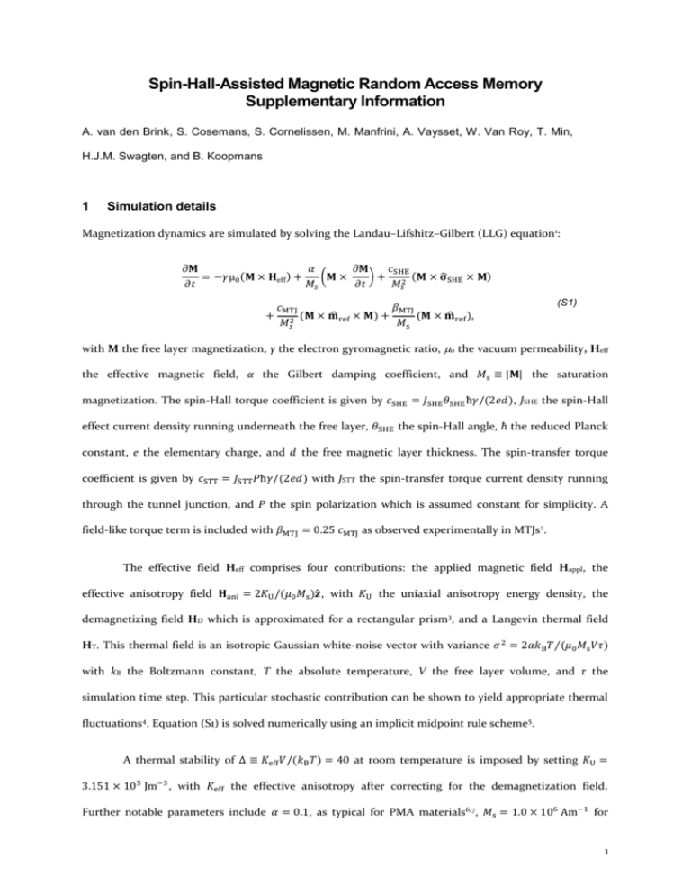
Spin-Hall-Assisted Magnetic Random Access Memory Supplementary Information A. van den Brink, S. Cosemans, S. Cornelissen, M. Manfrini, A. Vaysset, W. Van Roy, T. Min, H.J.M. Swagten, and B. Koopmans 1 Simulation details Magnetization dynamics are simulated by solving the Landau–Lifshitz–Gilbert (LLG) equation1: 𝜕𝐌 𝛼 𝜕𝐌 𝑐SHE = −𝛾µ0 (𝐌 × 𝐇eff ) + (𝐌 × ) + 2 (𝐌 × 𝛔 ̂SHE × 𝐌) 𝜕𝑡 𝑀𝑠 𝜕𝑡 𝑀𝑠 𝑐MTJ 𝛽MTJ (𝐌 × 𝐦 ̂ ref × 𝐌) + ̂ ref ), + 2 (𝐌 × 𝐦 𝑀𝑠 𝑀s (S1) with M the free layer magnetization, γ the electron gyromagnetic ratio, 0 the vacuum permeability, Heff the effective magnetic field, α the Gilbert damping coefficient, and 𝑀s ≡ |𝐌| the saturation magnetization. The spin-Hall torque coefficient is given by 𝑐SHE = 𝐽SHE 𝜃SHE ħ𝛾/(2𝑒𝑑), JSHE the spin-Hall effect current density running underneath the free layer, 𝜃SHE the spin-Hall angle, ħ the reduced Planck constant, e the elementary charge, and 𝑑 the free magnetic layer thickness. The spin-transfer torque coefficient is given by 𝑐STT = 𝐽STT 𝑃ħ𝛾/(2𝑒𝑑) with JSTT the spin-transfer torque current density running through the tunnel junction, and P the spin polarization which is assumed constant for simplicity. A field-like torque term is included with 𝛽MTJ = 0.25 𝑐MTJ as observed experimentally in MTJs2. The effective field Heff comprises four contributions: the applied magnetic field Happl, the effective anisotropy field 𝐇ani = 2𝐾U /(𝜇0 𝑀s )𝒛̂, with 𝐾U the uniaxial anisotropy energy density, the demagnetizing field HD which is approximated for a rectangular prism3, and a Langevin thermal field HT. This thermal field is an isotropic Gaussian white-noise vector with variance 𝜎 2 = 2𝛼𝑘B 𝑇⁄(𝜇0 𝑀s 𝑉𝜏) with kB the Boltzmann constant, T the absolute temperature, V the free layer volume, and τ the simulation time step. This particular stochastic contribution can be shown to yield appropriate thermal fluctuations4. Equation (S1) is solved numerically using an implicit midpoint rule scheme 5. A thermal stability of Δ ≡ 𝐾eff 𝑉/(𝑘B 𝑇) = 40 at room temperature is imposed by setting 𝐾U = 3.151 × 10⁵ Jm−3 , with 𝐾eff the effective anisotropy after correcting for the demagnetization field. Further notable parameters include 𝛼 = 0.1, as typical for PMA materials6,7, 𝑀s = 1.0 × 10⁶ Am−1 for 1 Co8, 𝜃SHE = 0.15 for Ta9, and P = 0.5. All simulations are carried out at T = 300 K, with the initial magnetization drawn from an appropriate Maxwell-Boltzmann distribution around 𝐌 = 𝑀s 𝒛̂. The Oersted field generated by JSHE is approximated by that of an infinite surface current, whereas Joule heating and current shunting effects are neglected. 2 Spin-Hall effect current pulse power consumption estimate In the main text, the power consumed by a 0.5 ns pulse of JSHE = 28 MA/cm2 is mentioned to be very small, at 9 fJ. This is based on a calculation in a simplified system: JSHE runs through a 4 nm thick β-Ta layer underneath the MTJ, which is 100 nm wide and 200 nm long, so that ISHE 0.112 mA. Given the typical resistivity value10 of 200 µΩ-cm for sputtered thin films of β-Ta, the resistance of the thin wire segment is 1 kΩ. Assuming the connecting wires and transistor contribute another 0.5 kΩ of resistance to the current path, the total resistance is estimated at 1.5 kΩ. The required driving voltage for the SHE pulse is thus 0.168 V, yielding an energy consumption of 9.4 fJ for a pulse of 0.5 ns. One could argue that additional capacitive losses in charging a separate line might affect the power consumption. This is difficult to quantify without an in-depth discussion of device integration, which is beyond the scope of this paper. However, a quick estimate shows that these losses are negligible compared to the static power consumption. Assuming each cell acts as a 1.8 fF capacitance (based on a 200 x 100 nm parallel plate capacitor with a dielectric constant of 10 and a separation of 1 nm) and 128 cells are addressed per line, the energy associated with charging a line (𝐸 = 0.5𝐶𝑉 2 ) is of the order of 10 fJ (STT pulse, unassisted), 1 fJ (STT pulse, assisted), or 0.1 fJ (SHE pulse), which in each case is negligible compared to the static write energy. Finally, it should be noted that there is a practical lower limit to the driving voltage, imposed by transistor operation requirements. Furthermore, in a practical implementation of SHE-accelerated STTMRAM, the device would likely be operated using a single voltage supply for both current pulses. Assuming a driving voltage of 0.9 V for both pulses increases the total power consumption to 0.32 pJ, which is still a factor 17 lower than the unassisted power consumption. 2 3 Parameter space exploration results As mentioned in the main text, an extensive study was performed regarding the general validity of the obtained results by systematically varying all relevant system parameters. These include ambient conditions (temperature, applied magnetic field), system properties (dimensions, magnetic anisotropy, saturation magnetization, damping, spin-Hall angle), and current pulse properties (current densities, pulse durations, and delay time). While varying each parameter, all other parameters are set to their default value as listed above and in the main text, unless stated otherwise. For each value of the parameter of interest, we generate a phase diagram of the switching probability Pswitch as a function of JSHE and JSTT. The number of averages per point is reduced to 64 for practical purposes. Typical examples of these phase diagrams are shown below where relevant. We extract two characteristic current densities from each phase diagram: the value of JSTT required to achieve Pswitch = 0.99 without SHE assistance, referred to as J0,STT, and the value of JSHE required to reduce JSTT to J0,STT/2 while maintaining Pswitch = 0.99, referred to as J½,SHE. This current density J½,SHE serves as a figure of merit describing the viability of the SHE-assisted write scheme for the given set of parameters. A lower value of J½,SHE indicates a more significant reduction in tunnel current density (and power consumption) using the SHE-assisted write scheme. 3 3.1 Temperature The effect of system temperature is illustrated by means of two phase diagrams, at T = 100 K (Figure 1a) and T = 1000 K (Figure 1b). Increasing system temperature is seen to reduce the value of J0,STT (see also Figure 2), which is explained by an increase in thermal fluctuations which reduces incubation delay. At higher temperatures, a higher value of JSHE is therefore required for the SHE pulse to offer a benefit over thermal fluctuations, as mentioned in the main text and observed in Figure 1b. The reduction in J0,STT also results in an increase of J½,SHE with temperature, as seen in Figure 2, indicating 20 0.8 0.8 15 0.6 0.6 10 0.4 5 0.2 sw itch 1 P STT 10 0.4 J J STT 15 1 P 20 (MA/cm2) (b) 25 (MA/cm2) (a) 25 sw itch that the SHE-assisted scheme becomes less effective with increasing temperature, as expected. 5 0 0 0 10 20 30 40 50 0.2 0 0 0 10 20 JSHE (MA/cm2) 30 40 50 JSHE (MA/cm2) Figure 1: Switching probability Pswitch out of 64 attempts as a function of the pulse current densities JSTT and JSHE, respectively, for a system temperature of (a) 100 K and (b) 1000 K. Current density (MA/cm2) 25 20 J0,STT J1/2,SHE 15 10 0 200 400 600 800 1000 Temperature Figure 2: Values of J0,STT (purple squares) and J½,SHE (orange circles) as a function of system temperature. Lines are a guide to the eye. 4 3.2 In-plane magnetic field As mentioned in the main text, application of a small magnetic field Bx (along the flow direction of JSHE) has a dramatic effect on the magnetization dynamics. Phase diagrams were created for a field range of 0 to 18 mT. The effective anisotropy field of the system is 28 mT; in-plane fields approaching this magnitude pull the magnetization significantly in-plane and cause precessions during the switching process. More importantly, for small values of Bx, the symmetry of the system is broken sufficiently to allow for directional switching without any STT current. This is clearly visible in the typical phase diagrams shown in Figure 3. The in-plane field also reduces the effective thermal stability of the system, however, reflected in an increase of J0,STT and a decrease of J½,SHE, shown in Figure 4. (b) 15 5 1 1 0.8 0.8 0.6 0.6 0.4 0 0 10 20 30 sw itch 5 0.2 0.2 0 P 0.4 sw itch 10 P STT (MA/cm2) 10 J J STT (MA/cm2) (a) 15 0 0 0 10 20 30 JSHE (MA/cm2) JSHE (MA/cm2) Figure 3: Switching probability Pswitch out of 64 attempts as a function of the pulse current densities JSTT and JSHE, for an in-plane magnetic field Bx of (a) 6 mT and (b) 12 mT. Current density (MA/cm2) 22 J0,STT 20 J1/2,SHE 18 16 14 12 10 8 -2 0 2 4 6 8 10 12 14 16 18 20 Bx Figure 4: Values of J0,STT (purple squares) and J½,SHE (orange circles) as a function of applied in-plane magnetic field. Lines are a guide to the eye. 5 3.3 Lateral dimensions To investigate the viability of the SHE-assisted scheme for different lateral dimensions, we simultaneously increase the bit length l and width w to maintain the same aspect ratio. This corresponds to a quadratic increase in the free layer volume V = d w l. The unassisted STT switching current density J0,STT is found to be constant under this variation (Figure 5a), corresponding to a quadratic increase in the critical current I0,STT = w l J0,STT (Figure 5b). This is in agreement with symmetry considerations. The spin-Hall current required to halve the required STT current is found to follow a quite different scaling behavior: it is independent of the lateral dimensions (Figure 5b). As I½,SHE = w de J½,SHE, with de the electrode thickness, this implies a 1/w dependence for J½,SHE, which is indeed observed in Figure 5a. This observed scaling behavior suggests that downscaling of SHE-assisted MRAM will pose a challenge. (b) 6 80 J0,STT 70 J1/2,SHE 60 50 40 30 I0,STT 5 Current (mA) Current density (MA/cm2) (a) 90 10*I1/2,SHE 4 3 2 20 1 10 0 0 100 200 300 Bit length, w = 0.5*l (nm) 0 100 200 300 Bit length, w = 0.5*l (nm) Figure 5: Values of (a) J0,STT (purple squares) and J½,SHE (orange circles) as a function of bit length, while maintaining a constant aspect ratio by proportionally scaling the bit width, and (b) corresponding currents. The spin-Hall current is scaled by a factor 10 for clarity. Lines are a guide to the eye. 6 3.4 Lateral dimensions with thermal stability constraint We explicitly study the lateral scaling behavior under constant thermal stability Δ = Keff 𝑉 𝑘B 𝑇 = 40, as such stable bits are interesting for memory applications. Reducing the free layer volume in this case requires an equivalent increase in the effective magnetic anisotropy Keff. Compared to the unconstrained scaling case discussed in the previous section, the STT switching current density is therefore expected to display an additional 1/(l x w) dependence, which is indeed observed (Figure 6). The spin-Hall current density is similarly affected, with J½,SHE approaching 100 MA/cm2 for a bit size of 80 x 40 nm, again demonstrating the challenge in downscaling SHE-based devices. (b) 10 J0,STT I0,STT J1/2,SHE I1/2,SHE Current (mA) Current density (MA/cm2) (a) 1000 100 10 1 0.1 0.01 0 100 200 300 Bit length, w = 0.5*l (nm) 0 100 200 300 Bit length, w = 0.5*l (nm) Figure 6: Values of (a) J0,STT (purple squares) and J½,SHE (orange circles) as a function of bit length, while maintaining a constant aspect ratio by proportionally scaling the bit width and a constant thermal stability by proportionally scaling the magnetic anisotropy constant, and (b) corresponding currents. Lines are a guide to the eye. 7 3.5 Aspect Ratio As mentioned in the main text, a ‘tail’ is observed in the phase diagram at high JSHE when using the default system parameters. This is mentioned to result from precessional motion around the inplane demagnetization field during the SHE pulse, implying that it should not occur in structures with an aspect ratio of 1. The phase diagrams shown in Figure 7 confirm these statements, showing no tail for an aspect ratio of 1 and an enhanced one for an aspect ratio of 50. The lowest value of J½,SHE is observed for an aspect ratio of 1 (Figure 8a), but a higher aspect ratio can be beneficial to reduce the SHE current (Figure 8b), and thus the Joule heating and power consumption, while maintaining thermal stability. 0.4 5 0.2 0.4 sw itch J 10 0.6 P 0.6 15 STT 10 0.8 sw itch (MA/cm2) 15 1 0.8 20 J STT (MA/cm2) 20 1 25 P (b) (a) 25 5 0 0 0 0 10 20 30 40 50 0.2 0 0 10 20 JSHE (MA/cm2) 30 40 50 JSHE (MA/cm2) Figure 7: Switching probability Pswitch out of 64 attempts as a function of the pulse current densities JSTT and JSHE, for an aspect ratio (l/w) of (a) 1 and (b) 50. The dimensions are chosen such that in each case the junction area is identical to that of the 200 x 100 nm junction, i.e. 141 x 141 nm and 1000 x 20 nm, respectively. (b) 10 20 Current (mA) Current density (MA/cm2) (a) 22 18 16 J0,STT 14 J1/2,SHE 1 I0,STT I1/2,SHE 0.1 12 10 0.1 1 10 Aspect Ratio (l/w) 100 0.01 0.1 1 10 100 Aspect Ratio (l/w) Figure 8: Values of (a) J0,STT (purple squares) and J½,SHE (orange circles) as a function of bit aspect ratio (w/l), and (b) corresponding currents. The area is constrained to 0.02 µm2 for each aspect ratio. Lines are a guide to the eye. 8 3.6 Free layer thickness Altering the magnetic free layer thickness, while constraining the thermal stability to Δ = Keff 𝑉 = 40, is found linearly affect both J0,STT and J½,SHE (Figure 9). Current density (MA/cm2) 𝑘B 𝑇 40 J0,STT J1/2,SHE 30 20 10 0.5 1.0 1.5 Free layer thickness (nm) Figure 9: Values of J0,STT (purple squares) and J½,SHE (orange circles) as a function of free layer thickness. The thermal stability is constrained to 40 for each thickness by adjusting the magnetic anisotropy. Lines are a guide to the eye. 3.7 Spin-Hall angle The spin-Hall angle θSH is defined as the ratio between the spin current Is and the electric current Ie in a material: 𝜃SH ≡ 𝐼s /𝐼e . It is therefore expected that J½,SHE is inversely proportional to θSH, which is exactly what is observed (Figure 10). Trivially, the value of J0,STT is not affected by θSH. Current density (MA/cm2) 60 J1/2,SHE 50 40 30 20 10 0 0.0 0.2 0.4 0.6 Spin-Hall Angle Figure 10: Value of J½,SHE as a function of the bottom electrode spin-Hall angle. The line is a guide to the eye. 9 3.8 Thermal Stability Increasing the thermal stability Δ = Keff 𝑉 𝑘B 𝑇 by increasing the effective magnetic anisotropy Keff is found to have a linear effect on J0,STT, as expected. The value of J½,SHE is similarly affected, but for low Current density (MA/cm2) thermal stability it saturates due to the diminishing role of JSHE compared to thermal fluctuations. 35 J0,STT J1/2,SHE 30 25 20 15 10 0 20 40 60 80 100 Thermal Stability Figure 11: Values of J0,STT (purple squares) and J½,SHE (orange circles) as a function of thermal stability. Lines are a guide to the eye. 3.9 Damping Changing the Gilbert damping parameter has a weak, linear effect on both J0,STT and J½,SHE (Figure 12). Both slightly increase with increasing damping. Current density (MA/cm2) 25 20 15 10 J0,STT J1/2,SHE 5 0.00 0.05 0.10 0.15 0.20 Gilbert damping constant Figure 12: Values of J0,STT (purple squares) and J½,SHE (orange circles) as a function of Gilbert damping parameter. Lines are a guide to the eye. 10 3.10 Saturation Magnetization Changing the saturation magnetization of the free layer has proportional effect on J0,STT and J½,SHE (Figure 13). For very low values of the saturation magnetization, the value of J½,SHE is seen to saturate, which is analogous to the effect of increasing system temperature to very high values. Current density (MA/cm2) 30 J0,STT J1/2,SHE 20 10 0 0.0 0.5 1.0 1.5 2.0 Saturation Magnetization (T) Figure 13: Values of J0,STT (purple squares) and J½,SHE (orange circles) as a function of free layer saturation magnetization. Lines are a guide to the eye. 3.11 Spin-Transfer Torque pulse duration The value of J0,STT decays rapidly as a function of the STT pulse length tSTT, as expected (Figure 14). It is interesting to observe, however, that J½,SHE depends only weakly on tSTT, indicating that the SHE-assisted scheme is still a viable alternative to unassisted switching in applications where longer switching times are allowed. Note the upturn in J½,SHE for small tSTT, which is due to tSTT ≤ tSHE. Current density (MA/cm2) 25 20 15 J0,STT J1/2,SHE 10 5 0 0 2 4 6 8 10 STT pulse duration (ns) Figure 14: Values of J0,STT (purple squares) and J½,SHE (orange circles) as a function of STT pulse duration. Lines are a guide to the eye. 11 3.12 Spin-Hall effect pulse duration Increasing the spin-Hall effect current pulse duration tSHE dramatically reduces the value of J½,SHE for tSHE < 0.3 ns (Figure 15). Further increases in tSHE have little effect. Herein, the spin-Hall effect pulse differs significantly from the STT pulse, due to the difference in spin orientation compared to the initial magnetization. The observed scaling demonstrates the usefulness of short SHE pulses, but also shows that reducing the current density by extending the SHE pulse duration is not an option. Current density (MA/cm2) 40 J1/2,SHE 30 20 10 0.0 0.2 0.4 0.6 0.8 1.0 SHE pulse duration (ns) Figure 15: Value of J½,SHE as a function of spin-Hall effect pulse duration. The line is a guide to the eye. 12 3.13 Delay between spin-Hall effect pulse and spin-transfer torque pulse Simultaneous application of two current pulses along two different current paths may prove impractical in actual devices. We therefore investigated the possibility of delaying the STT pulse. As shown in Figure 16, J½,SHE increases moderately with the delay time, showing little increase below tdelay = 1.5 ns. In fact, J½,SHE is significantly reduced (almost halved) if the two pulses are subsequent rather than simultaneous, as seen from the tdelay = 0.5 ns data point. In this case, the magnetization is maximally destabilized prior to STT current application, resulting in efficient switching. It should be noted, however, that the total switching time is then increased compared to the case of simultaneous pulses, skewing the comparison. Current density (MA/cm2) 50 J1/2,SHE 40 30 20 10 0 0 1 2 3 4 5 STT pulse delay time (ns) Figure 16: Value of J½,SHE as a function of the delay between the spin-Hall effect pulse and the spin-transfer torque pulse. A delay time of zero implies that both current pulses are started at t = 0. As the SHE pulse duration is 0.5 ns, the lowest value of J½,SHE is observed if the STT pulse is started immediately after the SHE pulse is ended. The line is a guide to the eye. 1 R. Koch, J. Katine, and J. Sun, Phys. Rev. Lett. 92 (8), 088302 (2004). A. M. Deac, A. Fukushima, H. Kubota, H. Maehara, Y. Suzuki, S. Yuasa, Y. Nagamine, K. Tsunekawa, D. D. Djayaprawira, and N. Watanabe, Nat. Phys. 4, 803–809 (2008). 3 A. Aharoni, J. Appl. Phys. 83 (6), 3432 (1998). 4 W. F. J. Brown, Phys. Rev. 130 (5), 1677–1686 (1963). 5 M. d’Aquino, C. Serpico, G. Coppola, I. D. Mayergoyz, and G. Bertotti, G., J. Appl. Phys. 99 (8), 08B905 (2006). 6 S. Mizukami, E. P. Sajitha, D. Watanabe, F. Wu, T. Miyazaki, H. Naganuma, M. Oogane, and Y. Ando, Appl. Phys. Lett. 96, 152502 (2010). 7 G. Malinowski, K. C. Kuiper, R. Lavrijsen, H. J. M. Swagten, and B. Koopmans, Appl. Phys. Lett. 94 (10), 102501 (2009). 8 L. Liu, O. Lee, T. Gudmundsen, D. C. Ralph, and R. A. Buhrman, Phys. Rev. Lett. 109 (9), 1–5 (2012). 9 L. Liu, C.-F. Pai, Y. Li, H. W. Tseng, D. C. Ralph, and R. A. Buhrman, Science 336 (6081), 555–558 (2012). 10 S. M. Rossnagel, J. Vac. Sci. Technol. B 20, 2328 (2002). 2 13


