Spintronics - Boston University Physics Department.
advertisement
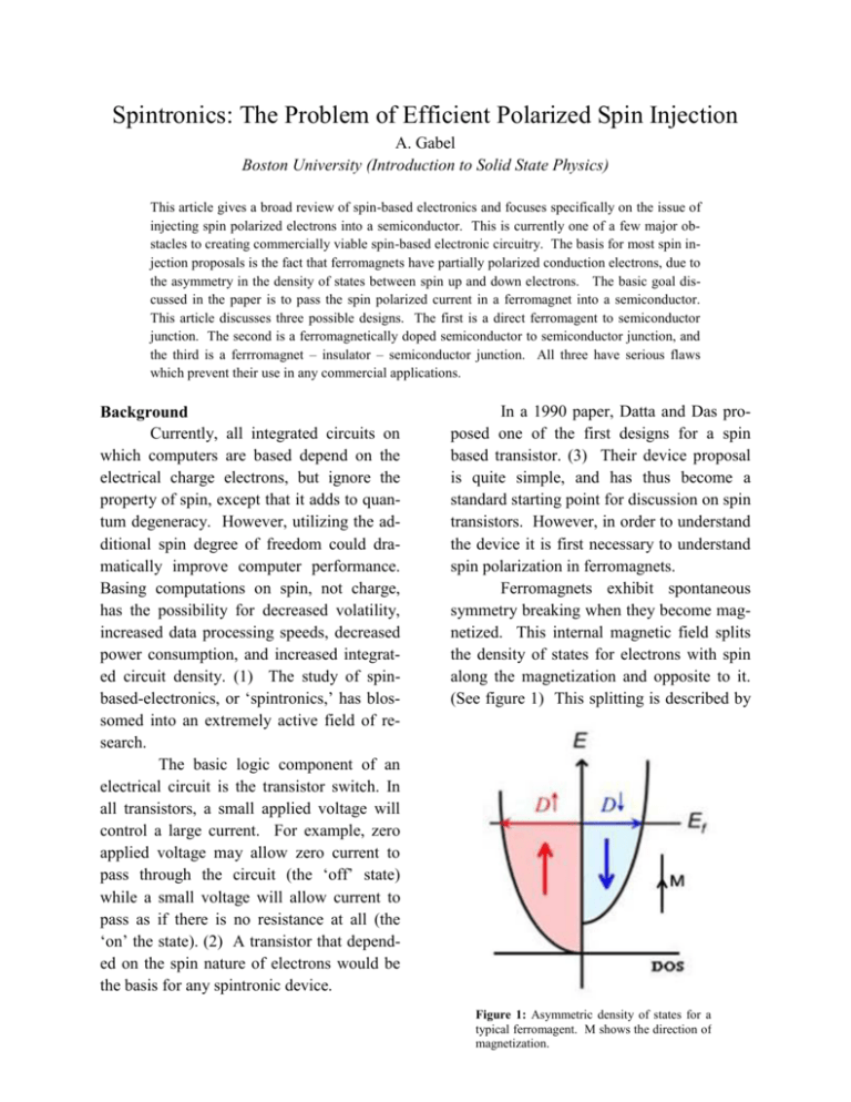
Spintronics: The Problem of Efficient Polarized Spin Injection A. Gabel Boston University (Introduction to Solid State Physics) This article gives a broad review of spin-based electronics and focuses specifically on the issue of injecting spin polarized electrons into a semiconductor. This is currently one of a few major obstacles to creating commercially viable spin-based electronic circuitry. The basis for most spin injection proposals is the fact that ferromagnets have partially polarized conduction electrons, due to the asymmetry in the density of states between spin up and down electrons. The basic goal discussed in the paper is to pass the spin polarized current in a ferromagnet into a semiconductor. This article discusses three possible designs. The first is a direct ferromagent to semiconductor junction. The second is a ferromagnetically doped semiconductor to semiconductor junction, and the third is a ferrromagnet – insulator – semiconductor junction. All three have serious flaws which prevent their use in any commercial applications. Background Currently, all integrated circuits on which computers are based depend on the electrical charge electrons, but ignore the property of spin, except that it adds to quantum degeneracy. However, utilizing the additional spin degree of freedom could dramatically improve computer performance. Basing computations on spin, not charge, has the possibility for decreased volatility, increased data processing speeds, decreased power consumption, and increased integrated circuit density. (1) The study of spinbased-electronics, or ‘spintronics,’ has blossomed into an extremely active field of research. The basic logic component of an electrical circuit is the transistor switch. In all transistors, a small applied voltage will control a large current. For example, zero applied voltage may allow zero current to pass through the circuit (the ‘off’ state) while a small voltage will allow current to pass as if there is no resistance at all (the ‘on’ the state). (2) A transistor that depended on the spin nature of electrons would be the basis for any spintronic device. In a 1990 paper, Datta and Das proposed one of the first designs for a spin based transistor. (3) Their device proposal is quite simple, and has thus become a standard starting point for discussion on spin transistors. However, in order to understand the device it is first necessary to understand spin polarization in ferromagnets. Ferromagnets exhibit spontaneous symmetry breaking when they become magnetized. This internal magnetic field splits the density of states for electrons with spin along the magnetization and opposite to it. (See figure 1) This splitting is described by Figure 1: Asymmetric density of states for a typical ferromagent. M shows the direction of magnetization. Figure 2: Schematic design of Datta and Das spin Transistor. Conductions would flow from left to right with initial polarization parallel to the direction of motion. The gate electrode is charged to block current and uncharged to allow current. the Zeeman effect. Polarization is defined as the fraction of uncompensated spin states at the Fermi surface. 𝑃𝑜𝑙𝑎𝑟𝑖𝑧𝑎𝑡𝑖𝑜𝑛 = | 𝐷(𝐸𝐹 )𝑢𝑝 − 𝐷(𝐸𝐹 )𝑑𝑜𝑤𝑛 | 𝐷(𝐸𝐹 )𝑢𝑝 + 𝐷(𝐸𝐹 )𝑑𝑜𝑤𝑛 The density of states at the fermi surface is proportional to the number of conduction electrons, so the polarization also gives the fraction of uncompensated spins of conducting charge carriers. The spin transistor proposed by Datta and Das depends on this polarization effect. The device would consist of a ferromagnetic source and a ferromagnetic drain electrodes with magnetization along the same direction for each. (4) These would be connected by a 2 dimensional semiconductor with a gate electrode placed in between. (See figure 2) A small voltage on the gate electrode will create an electric field, and for carriers confined to an asymmetric quantum well, this induces an effective magnetic field, called the Rashba field. (5) This magnetic field causes the electrons to precess. If the charge carriers precess to 180o out of phase then they will be anti-aligned with the drain electrode, and the impedence in the circuit will be large. However, if the carrier spins are aligned with the drain, then the impedence will be low. This device is a transistor since a small voltage on the gate electrode will control a relatively large current. There are four key ingredients to realize a working Datta and Das spin transistor. There must be successful injection of spin polarized current from the source electrode, spin coherent propagation through the semiconductor, induced spin precession, and spin-selective collection of current at the drain electrode. (5) All four are active areas of research, but this paper will focus on the first requirement, successful injection of polarized spin into the semiconductor. It is also important to note that this device would also work with a metal in place of the semiconductor. The motivation for using semiconductors is that they are already well studied and manufactured for integrated circuits with high purity and expertise. Optical Detection of Spin Injection Before discussing different spin injection designs, it is necessary to understand how to test experimentally if a current is polarized. Currently, the most sensitive technique uses optical methods. A typical set up is outlined below. In zincblende semiconductors, like GaAs, the selection rules for allowed recombination of electrons and holes are spin dependant. (5) The helicity or polarization of light coming from spin up electrons will be opposite that from spin down electrons. In a typical spin injection detection experiment (see figure 3) a GaAs/AlGaAs heterostructure is placed in contact with the semiconductor (GaAs) which is in contact with the ferromagnetic injector. When current is driven through the system, the electrons which have passed through the ferromagnet into the semiconductor layer combine with holes being driven by the current in the opposite direction. The light emitted from these recombinations will have polarization proportional to the polarization of the electrons, according to the spin-dependant recombination rules. By measuring the polarization of the emitted light, we can determine the spin polarization of the injected electron current. (6) Other current polarization techniques are often used which require only electronics and no optics, and are, thus, easier to implement. However, the optical technique is linearly sensitive to polarization, while other techniques are sensitive only to the polarization squared. (7) This is particularly useful since the effects being measured are often quite small. Spin Injection Schemes With a way to test a spin polarized injection mechanism, we now look at specific designs. The simplest design is that proposed by Datta and Das for their spin transistor. In there design, current is driven through a ferromagnet directly into a semiconductor. Unfortunately, experiment has shown that this injection technique has low efficiency, 1-2%. (8) This was explained with a theoretical framework by Schmidt et al, which assumes that the electrons propagate by diffusion. (9) The polarization of current at the interface is given by 𝑃= 𝑃0 1 + (1 − 𝑃02 ) 𝜎𝐹 𝜆𝑆𝐶 𝜎𝑆𝐶 𝜆𝐹 Where P0 is the polarization far inside the ferromagnet; σF and σSC are the conductivity of the ferromagnet and semiconductor, respectively; and λF and λSC are the mean distances travelled by spin carriers before a spin flipping scattering occurs. The important feature to notice in this equation is the ratio of conductivities in the denominator. Conducting ferromagnets, like Fe, typically have conductivities on the order of 103 greater than typical semiconductors. The huge number in the denominator drives the spin polarization to zero. This problem is referred to as ‘conductivity mismatch.’ It can only be overcome with a bulk ferromagnetic polarization, P0, at or extremely close to one. Then the otherwise large term in the Figure 3: Design for optical measuring polarization. Electrons are driven from top to bottom, where they recombine with holes, in the heterostructure to emit left or right circularly polarized light, depending on their spins. denominator is offset by the small (1-P02) factor. Unfortunately, the experimentally measured polarizations for some typical metals are far too low at 44% for Fe, 34% for Co, and 11% for Ni. (5) An alternative, which addresses the issue of ‘conductivity mismatch,’ is to use a ferromagnetically doped semiconductor in place of the ferromagnet. In this scenario, the conductivities of both materials are extremely close so the ratio of σF/σSC is close to 1. In fact, polarization of injected spins from a ferromagnetically doped semiconductor into an undoped semiconductor has been measured between 90-100%. (10) (11) However, this comes with some major limitations. A large external magnetic field (on the order of 1.5 Tesla) must be applied to achieve any appreciable polarization, P0. Also, the injection is only efficient at extremely low temperatures. The injected spin polarization drops to between 0-10% for temperatures above 40K. These limitations are substantial, and would preclude any commercially viable applications. There is another method which does not suffer from ‘conductivity mismatch’ or the need for extreme external fields and temperatures. It is an injector comprised of a ferromagent/insulator/semiconductor junction. Current would pass through the insulator from the ferromagnet to the semiconductor. Because the transport is due to a tunneling mechanism and not diffusion, our former analysis does not apply. This was first observed experimentally by Alvarado et al. for spin polarized electrons tunneling from a ferromagnetic STM tip, through vacuum, into a semiconductor sample. (12) Since then, experiment has detected polarizations across and a tunneling junction of up to 2% at room temperature (13) and as high as 30% polarization at temperature of 5K. (14) A theoretical framework has been worked out that predicts the spin injector efficiency will increase, as the insulator or barrier layer increases in thickness. (1) But a larger barrier leads to greater impedence in the circuit. So employing a tunneling junciton for spin injection implies a trade-off. One can achieve high polarization efficiency at the cost of either a low current density in the semiconductor or the need for a high current density in the ferromagnet. These are not ideal characteristics for in integrated circuit. Conclusions The use of spin in electronic circuitry is a tantalizing method to increase computer performance. But so far, this has only been realized as a vague theory, not in actual application. The spin transistor was first proposed by Datta and Das close to 20 years ago, and a working model has never been successfully built. High efficiency spin injection is definitely an obstacle, and so far all of the proposed solutions have been lacking. The three specific injection systems discussed in this paper have serious drawbacks in their present form which would preclude them from useful applications. There are still many new ideas that this paper did not address, and these may be the key to unlocking the spin transistor puzzle. Whether spintronics is possible is still an open question. References 1. Spintronics: A Spin-Based Electronics. S. A. Wolf, D. D. Awschalom, R. A. Buhrman, J. M. Daughton, S. von Molna. November, 2001, Science, Vol. 294, p. 1488. 2. Woodford, Chris. Transistors. Explain That Stuff. [Online] September 10, 2008. [Cited: April 25, 2009.] http://www.explainthatstuff.com/howtransistorswork.html. 3. Electronic Analog of Electro-optic Modulator. S. Datta, B. Das. 7, s.l. : Applied Physics Letters, February 1990, Vol. 56. 4. Spintronics. Sarma, Sankar Das. Nov-Dec 2001, American Scientist, Vol. 89, pp. 516-523. 5. D.D. Awschalom, D. Loss, N. Samarth. Semiconductor Spintronics and Quantum computation. Germany : Springer, 2002. 6. Spin Injection into Semiconductors. M. Oestreich, J. Hubner, D. Hagele, P. J. Klar, W. Heimbrodt, W. W. Ruhle, D. E. Ashenford, B. Lunn. 9, s.l. : Applied Physics Letters, 1999, Vol. 74. 7. Johnson, M. Spin Physics in Semiconductors. [ed.] M. Dyakonov. Berlin : Springer, 2008. p. 297. 8. Observation of Spin Injection at a Ferromagnet-Semiconductor Interface. P. R. Hammar, B. R. Bennett, M. J. Yang, M. Johnson. 1, s.l. : Physical Review Letters, 1999, Vol. 83. 9. Fundamental obstacle for electrical spin injection from a ferromagnetic metal into a diffusive semiconductor. G. Schmidt, D. Ferrand, L. W. Molenkamp. 8, s.l. : Physical Review B, 2000, Vol. 62. 10. Electrical spin injectin in a ferromagnetic semiconductor heterostructure. Y. Ohno, D. Young, B. Beschoten, F. Matsukura, H. Ohno, D. Awschalom. s.l. : Nature, 1999, Vol. 402, p. 790. 11. Injection and detection of a spin-polarized current in a lightemitting diode. R. Fiederling, M. Keim, G. Reuscher, W. Ossau, G. Schmidt, A. Waag, L. Molenkamp. s.l. : Nature, 1999, Vol. 402, p. 787. 12. Obsevation of spin-polarized-electron tunneling from a ferromagnet into GaAs. S. Alvarado, P. Renaud. 9, s.l. : Physical Review Letters, 1992, Vol. 68. 13. Room-temperature spin injection from Fe into GaAs. H. Zhu, M. Ramsteiner, H. Kostial, M. Wassermeier, H. Schonherr, K. Ploog. 1, s.l. : Physical Review Letters, 2001, Vol. 87. 14. Electrical spin-injection into silicon from a ferromagentic metal/tunnel barrier contact. B. Jonker, G. Kioseoglou, A. Hanbicki, C. Li, P. Thompson. s.l. : Nature physics, 2007, Vol. 3, p. 542. 15. Reexamination of some spintronic field-effect device concepts. S. Bandyopadhyaya, M. Cahay. 8, s.l. : Applied Physics Letters, August 2004, Vol. 85, p. 1433. 16. Spin-Dependent Tunneling into Ferromagnetic Nickel. P.M. Tedrow, R. Meservey. F, s.l. : Physical Review Letters, January 1971, Vol. 26.
