Lecture 9
advertisement
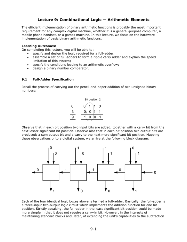
Lecture 9: Combinational Logic — Arithmetic Elements The efficient implementation of binary arithmetic functions is probably the most important requirement for any complex digital machine, whether it is a general-purpose computer, a mobile phone handset, or a games machine. In this lecture, we focus on the hardware implementation of basic binary arithmetic functions. Learning Outcomes: On completing this lecture, you will be able to: specify and design the logic required for a full-adder; assemble a set of full-adders to form a ripple carry adder and explain the speed limitation of this system; specify the conditions leading to an arithmetic overflow; design a binary number comparator. 9.1 Full-Adder Specification Recall the process of carrying out the pencil-and-paper addition of two unsigned binary numbers: Bit position 2 6 3 9 0 1 1 0 01 01 1 1 1 0 0 1 Observe that in each bit position two input bits are added, together with a carry bit from the next lesser significant bit position. Observe also that in each bit position two output bits are produced; a sum output bit and a carry to the next more significant bit position. Mapping these observations onto a digital system, we arrive at the following block diagram: 0 1 0 0 1 0 1 1 0 1 1 0 1 0 0 0 1 Each of the four identical logic boxes above is termed a full-adder. Basically, the full-adder is a three-input two-output logic circuit which implements the addition function for one bit position. Strictly speaking, the full-adder in the least significant bit position could be made more simple in that it does not require a carry-in bit. However, in the interests of maintaining standard blocks and, later, of extending the unit’s capabilities to the subtraction 9-1 of 2’s complement numbers, we prefer to keep a standard full-adder in the least significant bit position. 9.2 Full-Adder Design A B Cout Cin S By considering all the possible bit combinations for the inputs to a full-adder, designated A, B, and Cin, we arrive at the following truth table for the output variables S, denoting the sum output bit, and Cout, denoting the carry to the next more significant bit position: A 0 0 0 0 1 1 1 1 B 0 0 1 1 0 0 1 1 Cin 0 1 0 1 0 1 0 1 Cout 0 0 0 1 0 1 1 1 S 0 1 1 0 1 0 0 1 B 1 A 1 1 1 Cin We note from the Karnaugh map for S, shown above, that no simplification is possible. The resulting equation may, however, be manipulated to yield: S AB Cin ABC in AB C in ABC in A B Cin BC in A B C in BC in AB C in AB C in A B Cin 9-2 B 1 A 1 1 1 Cin The Karnaugh map for Cout, above, leads to the equation Cout AB BC in Cin A However, noting the necessity for the exclusive-OR function in the equation for S, we can reformulate Cout to give B 1 A 1 1 1 Cin C out AB AB Cin ABC in AB Cin AB AB AB Cin A B Hence, assuming the availability of Exclusive-OR gates, we have the following logic diagram for the full-adder: A B S Cout Cin 9-3 9.3 Ripple Carry Architecture Once we have a full-adder block designed, we can then assemble full-adders into a complete system for the addition of binary numbers of any size. For example, the following system represents the logic required to add two four-bit binary numbers: A3 A1 A2 B3 B2 C3 C4 S3 A0 B1 C2 S2 B0 C1 S1 C0 S0 Because of the way by which the carry has to “ripple” from one full-adder to the next, the system is termed a ripple carry architecture. The main positive feature of this architecture is its simplicity. It does, however, have severe speed limitations. We have previously noted that in a multilevel logic circuit, delays accumulate as a signal flows from level to level. The ripple carry circuit is essentially a multilevel logic circuit; before the calculation can properly begin in bit position 3, delays affecting C3 must be complete; before the calculation can properly begin in bit position 2, delays affecting C2 must be complete, etc. Clearly the overall propagation delay is directly proportional to the wordsize of the input binary numbers. For three or four-bit binary numbers, the delay would be comparable to that of any logic circuit with which we have dealt. However, today’s microprocessors feature 64-bit binary numbers and the associated delay in a ripple carry adder would be incompatible with true high speed operation. Different architectures have to be employed, in particular those based on the socalled carry-lookahead principle — most of the system comprises the ripple carry configuration but some regularly spaced intermediate carries such as C 4, C8, C12, C16, etc are directly generated from the input variables. Complexity is significantly increased but a speedier system results. 9.4 Overflow As previously pointed out, all digital machines have a finite range of possible arithmetic values due to the limited number of bits available for representing numbers. When binary numbers are subject to arithmetic operations such as addition, it is possible to exceed the available bit capacity, ie an overflow can be generated. It is important that an overflow condition be flagged. We illustrate the detection conditions for overflow by means of examples for four-bit numbers: (i) Unsigned Binary: With N = 4, the valid representation range is 0 through to 15 9-4 No Overflow 3 10 13 Overflow 0 0 1 1 01 0 0 1 1 0 1 1 0 1 7 10 1 0 1 1 1 111 01 1 0 0 0 0 1 We observe: if C 4 0 then no overflow if C 4 1 then overflow Thus, the carry out from the most significant bit position can be used as an overflow flag. (ii) Signed 2’s Complement: Again with N = 4, the valid representation range is from -8 through to +7 +3 +4 +7 No Overflow 0 0 1 1 00 0 1 0 0 0 0 0 0 0 0 1 +5 +4 -7 Overflow 0 1 0 1 001 10 00 00 1 0 0 1 -3 -4 -7 1 1 0 1 11 1 1 0 0 0 0 0 1 0 0 1 -5 -4 +7 1 0 1 1 110 10 00 00 0 1 1 1 There are two mechanisms that can be used to detect an overflow: (a) If the operand sign bits are the same but differ from the sign bit of the result. (b) If the most significant carry out, C4, is different from the carry in to the most significant bit position, C3. Both of these conditions can be encapsulated in appropriate Boolean equations. 9.5 The Comparator This very important logic circuit is used for detecting the equivalence of two input binary numbers. 9-5 AN-1 A0 E BN-1 B0 With A AN 1 A1 A0 and B BN 1 B1 B0 representing two input binary numbers AB then E 1 if Consider first the case of single-bit numbers, N = 1: A0 0 0 1 1 B0 0 1 0 1 E 1 0 0 1 From the truth table we have E A0 B0 A0 B0 A0 B0 ie an Exclusive-NOR gate is required. Now consider the case of two-bit numbers. The following truth table applies: A1 0 0 0 0 0 0 0 0 1 1 1 1 1 1 1 1 A0 0 0 0 0 1 1 1 1 0 0 0 0 1 1 1 1 B1 0 0 1 1 0 0 1 1 0 0 1 1 0 0 1 1 9-6 B0 0 1 0 1 0 1 0 1 0 1 0 1 0 1 0 1 E 1 0 0 0 0 1 0 0 0 0 1 0 0 0 0 1 B1 1 1 A0 1 A1 1 B0 The Karnaugh map implies that no simplification is possible. However, the diagonal line of 1’s suggests that an Exclusive-OR function may be present: E A1 A0 B1 B0 A1 A0 B1 B0 A1 A0 B1 B0 A1 A0 B1 B0 A1 B1 A0 B0 A0 A1 A1 B1 A0 B0 A0 B0 A1 B1 A1 B1 A0 B0 A0 B0 A1 B1 A0 B0 or, putting it in words: E 1 if ( A1 B1 ) AND ( A0 B0 ) A corresponding logic diagram is shown. A1 B1 E A0 B0 9.6 Conclusion We have given an introductory treatment of logic circuits for arithmetic operations. A fulladder has been defined and designed and it has been shown how to assemble a number of full-adders to form a ripple-carry adder. The speed limitations of the ripple carry architecture have been noted. Logic for detecting overflow conditions and for comparing binary numbers has been considered. 9-7
