DAAC proposal
advertisement
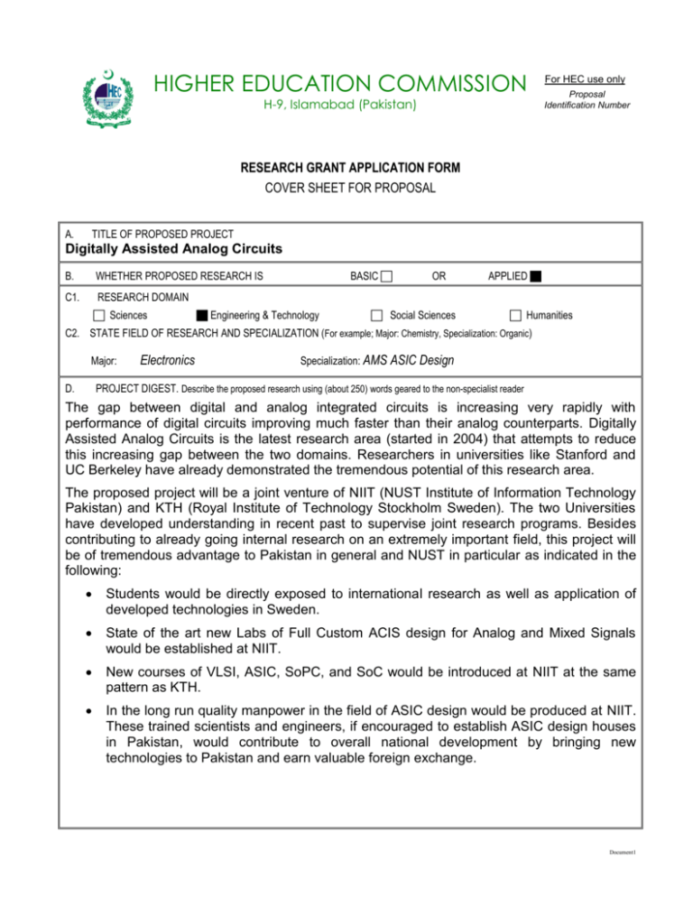
HIGHER EDUCATION COMMISSION H-9, Islamabad (Pakistan) For HEC use only Proposal Identification Number RESEARCH GRANT APPLICATION FORM COVER SHEET FOR PROPOSAL A. TITLE OF PROPOSED PROJECT Digitally Assisted Analog Circuits B. WHETHER PROPOSED RESEARCH IS C1. RESEARCH DOMAIN Sciences BASIC Engineering & Technology OR Social Sciences APPLIED Humanities C2. STATE FIELD OF RESEARCH AND SPECIALIZATION (For example; Major: Chemistry, Specialization: Organic) Major: D. Electronics Specialization: AMS ASIC Design PROJECT DIGEST. Describe the proposed research using (about 250) words geared to the non-specialist reader The gap between digital and analog integrated circuits is increasing very rapidly with performance of digital circuits improving much faster than their analog counterparts. Digitally Assisted Analog Circuits is the latest research area (started in 2004) that attempts to reduce this increasing gap between the two domains. Researchers in universities like Stanford and UC Berkeley have already demonstrated the tremendous potential of this research area. The proposed project will be a joint venture of NIIT (NUST Institute of Information Technology Pakistan) and KTH (Royal Institute of Technology Stockholm Sweden). The two Universities have developed understanding in recent past to supervise joint research programs. Besides contributing to already going internal research on an extremely important field, this project will be of tremendous advantage to Pakistan in general and NUST in particular as indicated in the following: Students would be directly exposed to international research as well as application of developed technologies in Sweden. State of the art new Labs of Full Custom ACIS design for Analog and Mixed Signals would be established at NIIT. New courses of VLSI, ASIC, SoPC, and SoC would be introduced at NIIT at the same pattern as KTH. In the long run quality manpower in the field of ASIC design would be produced at NIIT. These trained scientists and engineers, if encouraged to establish ASIC design houses in Pakistan, would contribute to overall national development by bringing new technologies to Pakistan and earn valuable foreign exchange. Document1 E1. PRINCIPAL INVESTIGATOR NAME (full with no initials) Dr Nasir-ud-Din Gohar E4. DEPARTMENT/SECTION Communication Systems Engineering E7. E5. UNIVERSITY/INSTITUTION NUST Institute of Information Technology (NIIT) Telephone: +92-51-928-0229 Fax: +92-51-928-0658 (Area code, number and extension) (Area code, number) E2. HIGHEST DEGREE E3. POSITION/TITLE PhD HoD/Professor E6. MAILING ADDRESS 166-A, St#9, Chaklala Scheme III, Rawalpindi, Pakistan. Email: ndgohar@niit.edu.pk F: CO-PRINCIPAL INVESTIGATOR Name & Position Professional Address Dr. Arshad Ali (DG NIIT) 166-A St#9, Chaklala Scheme III, Rawalpindi, Pakistan G1. PROPOSED DURATION OF PROJECT: (in months) 36 months G2. PROPOSED STARTING DATE H. TOTAL FUNDS REQUESTED 1st September 2007 or after with Approval from HEC, Pakistan Rs. 5.914 million CERTIFICATES 1. 2. 3. Certified that the equipment(s) demanded for the subject project is / are not available in the University / Institute. Certified that the project under reference has not been submitted to any other funding agency including HEC. Certified that No portion of the project has been funded by any other funding agency including HEC in the past. SIGNATURE OF PRINCIPLE INVESTIGATOR SIGNATURE OF THE HEAD OF INSTITUTION (Vice-chancellor / Rector of University, Director of degreeawarding Institutions) ENDOSEMENT OF THE HEAD OF INSTITUTION (Vice-chancellor/Rector of University, Director of Degree-awarding Institutions) SIGNATURE OF PRINCIPAL INVESTIGATOR Signature & Date Date SINATURE OF CO-PRINCIPAL INVESTIGATOR Date Name Maj Gen Muhammad Asghar Title: Rector Address: NUST HQ Tamiz-ud-Din Road, P.O. Box 297, Rawalpindi, Pakistan Phone +92 51 927 1978 E-mail: registrar@nust.edu.pk 2 FAX +92 51 927 1577 PROJECT DETAILS 1. PROJECT SUMMARY Describe the proposed research using (about 250) words. Digitally Assisted Analog Circuits is the latest research area (started in 2004) that attempts to reduce the increasing gap between the advancement of digital and analog integrated circuits. During the last 15 years increase in the performance of digital ICs has become 150 times more than their analog counterparts. Since any real world system must compose of analog components, slow advancement of analog integrated circuits is now actually hindering the development of digital electronics. If these trends continue to occur, this problem is likely to become worse in the near future. Digitally Assisted Analog Circuits is a recently proposed method that has tremendous potential to nullify this effect. Basic idea is to simplify the analog circuits at the cost of decreased precision. This loss in precision is then modeled and compensated in the digital domain. The project will be executed simultaneously at NIIT and KTH for a period of approximately 03 years. Main aim is to apply this scheme in wireless technology and simplify the analog circuitry of existing technology improving its performance parameters like area, speed and power.01 PhD and 02 master students will be trained along with the central focus of establishment of SoC Labs and new courses. The completion of PhD degree will take more than 03 years (Minimum PhD degree time in Sweden is 04 years with average time between 4.5 to 5 years). 2. PROPOSED GOALS/OBJECTIVES (please identify quantifiable goals) i. If the proposed research is basic, please identify or postulate scientific hypothesis on which your proposed goal is based. ii. If the proposed research is applied, please clearly identify the output in the form of a product or process, need or relationship to industry and also identify the end-user of your output/ product. P.I. is encouraged to make preliminary inquiries with the proposed end user and attach any certificate/ document in support of the proposed research. HYPOTHESIS/BASIS OF RESEARCH (if basic research) N/A GOALS/OBJECTIVES (please quantify your objectives in case of Applied research) 1. To contribute to electronics/IC industry by providing a solution to the rapidly increasing problem of gap between analog and digital domains 2. To improve the performance of existing wireless electronics (speed, area, power) by application of digitally assisted analog circuit technology 3. To provide to faculty and students at NIIT, exposure to international research and state of the art technology (This will include direct training (01PhD and 02 MS students) and indirect training (Workshops by KTH faculty, New courses at undergrad / grad levels) 4. To establish advanced VLSI (Full Custom Digital and AMS design) labs at NIIT 3 5. To introduce new courses of SoC, VLSI and ASIC design in NUST at grad/undergrad levels 6. To produce quality manpower in the field of Full Custom ASIC design and help in establishing ASIC design houses in Pakistan IDENTIFY END USER/ BENEFICIARY INDUSTRY (if applied research) Electronics Industry IC Industry Telecom Industry 3. INTRODUCTION (not to exceed one page) The introduction should consist of three paragraphs; the first paragraph should indicate the scientific hypothesis/commercial basis on which the project is based. The second paragraph should introduce the precise nature of the project, and the final paragraph should indicate the proposed objectives in the light of the first two paragraphs and explain clearly what the reader will see in the main body of the proposal. (PLEASE ATTACH ONE SHEET ONLY) (Pl. see annexure-A) 4A. BACKGROUND OF THE RESEARCH PROBLEMS TO BE ADDRESSED (Not to exceed two pages) i. In case of basic research, a comprehensive and up-to-date literature survey clearly highlighting the existing gaps and what new information will be added to the existing pool of knowledge. ii. In case of applied research, please also identify the industry in Pakistan, which should benefit from the process/product. Please justify how the proposed research will contribute to the national economy/social sector. Please justify your claim by giving figures of import/export, present market, future trends etc. The principal Investigator is encouraged to discuss the proposed research with the proposed beneficiary and attach supporting documentation. (PLEASE ATTACH TWO SHEETS ONLY) (Pl. see annexure -B) 4B. RESEARCH PLAN: SCHEDULE/PHASING (Not to exceed one page) (PLEASE ATTACH ONE SHEET ONLY) (Pl. see annexure -C) 4C. REFERENCES (cited in 3, 4A & 4B; not to exceed two pages) (PLEASE ATTACH TWO SHEET ONLY) (Pl. see annexure -D) 4 5. IMPACT (of proposed research on teaching/training of manpower, institutional capability building and on local industry) National / International electronics/IC industry would be benefited by providing a solution to the rapidly increasing problem of gap between analog and digital domains. Performance of existing wireless electronics (speed, area, power) would improve by application of digitally assisted analog circuit technology. Faculty and students at NIIT, will be exposed to international research and state of the art technology. Advanced VLSI (Full Custom Digital and AMS design) labs will be established at NIIT. New courses of SoC/SoPC, VLSI and ASIC design will be introduced in NIIT at grad/undergrad levels. Quality manpower in the field of Full Custom ASIC design will be produced and will help in establishing ASIC design houses in Pakistan. 6. COLLABORATING LABS In case of collaboration with national/international research group or local industry, please identify clearly the parts of research that will be carried out in the participating laboratories and please identify complimentarily and/or justify the need for collaboration) P.I.s are encouraged to find collaborating partners within Pakistan, particularly in less developed areas. Include a letter from Collaborating agency expressing willingness to collaborate. Royal Institute of Technology (KTH), Stockholm, Sweden-SoC Design Lab NUST Institute of Information Technology (NIIT), Rawalpindi -FPGA System Design Lab 7. FACILITIES AND FUNDING 7A. Facilities: equipment available for the research project IN THE HOST UNIVERSITY/INSTITUTION NIIT Library NIIT digital database NIIT FPGA System Design Lab 7B. Scientific Personnel Available 02 Professors 01 PhD Student 5 Required* 02 Master Students *Involvement of research students is encouraged. 7C. Other funding available for the proposed studies (if any) N/A 8. PRINCIPAL INVESTIGATOR A brief resume of research accomplished in the last 05 years. Please specify title of the research proposal(s), duration, funding source(s) and award amount(s). (Pl. see annexure -E) 8. PRINCIPAL INVESTIGATOR: continued 1. 2. 3. Please attach C.V. Number of Publications during the last five years & page numbers on the C.V. where these publications are listed Number of research projects completed & page number where this information appears National: 03 Please see pages: 8-10 of CV International: 34 Please see pages : 8-10 of CV Basic: _________ Please see pages ___________ of CV Applied 36 Please see pages: 8-10 of CV 9A. ESTIMATED BUDGET FOR THE PROPOSED RESEARCH PERIOD DESCRIPTION A. Salaries and Honorarium PI: One month/year of basic salary @ Co-PI: One month basic salary for the entire duration % of time devoted to Project YEAR 1 10% 0.1 YEAR 2 YEAR 3 0.1 5% Amount (in million Rs.) 0.1 0.3 0.15 0.15 1.056 @ PhD Student-1 * MS Student-1 ** MS Student-2 ** 75% 0.008 x 12 0.008 x 12 0.072 x 12 = 0.096 = 0.096 = 0.864 0.008 x 12 0.008 x 6 = 0.096 = 0.048 0.008 x 12 0.008 x 6 = 0.096 = 0.048 6 0.144 0.144 Subtotal: B. 0.538 0.292 1.794 Permanent Equipment (Please attach invoice/quotation and expected delivery date for items costing over Rs. 0.1 million.) Full Custom ASIC design lab equipment (Workstations) 2 x 0.05 0.5 Full Custom ASIC design lab equipment (Software Tools)* Subtotal: *Quotations attached in Annexure-G C. 0.964 0.1 1.0 0.6 1.0 1.1 Expendable supplies Subtotal: 9A. ESTIMATED BUDGET FOR THE PROPOSED RESEARCH PERIOD (continued) DESCRIPTION YEAR 1 YEAR 2 YEAR 3 D. Others D1. Literature, documentation, information, online literature search, contingencies, postage, etc. Documentation, Stationary etc. Subtotal: D2. Amount (in million Rs.) 0.05 0.05 0.05 0.15 0.05 0.05 0.05 0.15 0.4 0.4 0.2 1.0 Local Travel (Destination and Purpose) KTH Visit 7 Conference/Journal recitation 0.5 0.5 1.0 0.7 2.0 Audit Fee (Max. Rs 10,000) 0.01 0.01 Accountant Fee (Max. Rs. 10,000) 0.01 0.01 0.7 0.7 Subtotal: D3. 0.9 0.4 Miscellaneous KTH tuition fee Subtotal: 0.72 Subtotal (D1 + D2 + D3): 0.97 0.45 1.45 2.87 E. Indirect cost (University overheads) 0.05 0.05 0.05 0.15 1.658 1.792 2.464 5.914 02 % of Total direct cost to meet office support, utilities, etc. Grand Total (A + B + C + D+E): 9B. JUSTIFICATION (Please justify your request in a background of the existing facilities available at the host Institute.) A. Salaries & Allowances (All positions, other than PI and Co-PI, must be fully justified. Please give qualifications/requirements of each of the new full-time positions requested for in the Proposal.) There will be 02 MS and 01 PhD students who will be working directly for this project. Funding is required for the stipends of these students B. Permanent Equipment (Please identify major items (over Rs. 25,000). Major pieces of equipment costing over Rs. 0.1 million must be fully justified. Minor items (under Rs. 25,000) may be lumped into one.) C. Software is required for the Full Custom ASIC Design Lab, an extension of existing FPGA Lab. Other major permanent items for lab are workstations. Expendable supplies N/A D. Other Costs. (Travel must be justified.) Traveling to and from KTH is extremely necessary in order to have combined reviews after each milestone and finalize the future strategies. 8 ANNEXRE-A INTRODUCTION Scientific / Commercial Basis In past decades, “Moore’s law” has governed the revolution in microelectronics. Through continuous advancements in device and fabrication technology, the industry has maintained exponential progress rates in transistor miniaturization and integration density. As a result, microchips have become cheaper, faster, more complex, and more power efficient. However, digital performance metrics have grown significantly faster than corresponding measures for analog circuits, especially ADCs (analog-to-digital converters). Since most DSP (digital signal processor) projects depend on A/D conversion in the interfaces, this growing disparity in relative performance increase has the potential to threaten the rate of progress of DSP hardware. Much of the performance gain in digital hardware can be traced to corresponding advances in integrated circuit technology. For example, over the past 30 years we have witnessed a steady decrease in transistor channel length by two orders of magnitude from 10µm in 1970 to less than 0.1µm today. While this reduction of feature size benefits analog and digital circuits alike, overall analog circuit performance is compromised by other trends such as reduced supply voltages. While analog and digital system performance increases exponentially over time, microprocessor performance increased more than a thousand fold compared with an increase of only 10 times for ADCs. As the relative performance gap widens, applications such as digital audio, video, and RF (radio frequency) communication are increasingly limited not by the available digital processing power, but by their analog interfaces. The digitally assisted analog circuits avoid such trade-offs by delegating analog precision requirements to a digital processor. The relaxed analog requirements translate into improved metrics such as reduced power dissipation or increased speed. Key to this approach is a statistical system identification technique that continuously monitors analog imperfections. Judicious selection of the algorithms employed in the digital processor translates into a negligible area and power penalty from the DSP that further benefits from the continued technology scaling. Nature of Project The project is directly aimed at beginning research in the field of digitally assisted analog integrated circuits in Pakistan. 01 PhD and 02 MS students would be trained from NIIT and Pakistan. The total duration of the project is estimated to be 03 years. However, as mentioned earlier, completion of PhD degree in Sweden requires a minimum of 04 and an average of 05 years. Along with this central focus, this project will result in development of advanced ASICs labs at NIIT, introduction of new courses at grad/ undergrad levels and exposure of NIIT students to latest international research. 9 Objectives As discussed earlier, the objectives of the project are: 1. To contribute to electronics/IC industry by providing a solution to the rapidly increasing problem of gap between analog and digital domains. 2. To improve the performance of existing wireless electronics (speed, area, power) by application of digitally assisted analog circuit technology. 3. To provide to faculty and students at NIIT, exposure to international research and state of the art technology (This will include direct training (01 PhD and 02 MS students) and indirect training (Workshops by KTH faculty, New courses at undergrad / grad levels). 4. To establish advanced VLSI (Full Custom Digital and AMS design) labs at NIIT. 5. To introduce new courses of SoC, VLSI and ASIC design in NUST at grad/undergrad levels. 6. To produce quality manpower in the field of Full Custom ASIC design and help in establishing ASIC design houses in Pakistan. 10 ANNEXRE-B BACKGROUND AND METHODOLOGY Background As stated in introduction, this work will have a direct contribution to the current flow of international microelectronics and Telecom industry. Unfortunately in Pakistan, these industries are almost nonexistent. A major impact of this project will be development of quality manpower in Pakistan in the fields of Full Custom ASIC design during the course of this project. If proper guidance and opportunities are provided, the trained people from this project will be encouraged to open ASIC design houses in Pakistan. As can be seen in the next figure, the gap between trained manpower requirements and actually available manpower in the microelectronics industry is on a significant increase. This clearly indicates that there is a tremendous potential of business and jobs in the field of ASIC design since the industry is already deficient of trained manpower. Hence if people could be trained in this field, it will open new doors of opportunities in Pakistan to generate revenue as well as enter the highway of state of the art technologies. Also this project is not a typical research project with limited beneficiaries. Along with helping to establish local industry of ASIC design, this project will result in providing an invaluable exposure of 11 faculty and students of NUST to modern international research and development. This will in turn help in improving the overall standards and educational quality at our local universities. Methodology As stated earlier, this project will be executed in a span of 03 years. Year-1 will start with initial study and concepts and formal enrollment of PhD students. KTH advisor will be invited to NIIT Pakistan and an SoC workshop will be conducted for faculty and students of NIIT. First conference paper will be published by the end of year followed by visit to KTH for progress review and planning for future. An introductory course of VLSI will be started at undergrad level at NIIT. In year-2 exact research problem will be formulated and second paper regarding the problem and proposed solution will be published. Tools for Full Custom ASIC design (Layout editor, Design Rule Checker, Simulator etc) would be procured and Infrastructure for the lab will be established. A second course of advance VLSI will be started at grad and undergrad level at NIIT. MS students will also be registered and will complete their course work. This will be followed by visit to KTH for progress review and future planning. In year-3 the PhD student will shift to Sweden to complete the rest of research at KTH labs. Physician design will be implemented and the paper of design implementation will be published. Feasibility of establishment of first Full Custom ASIC design house in Pakistan will be made. MS students will complete their thesis and degree. Year will end up with visit to KTH for progress review and future planning to establish first full custom ASIC design house with human resource trained and produced at NIIT. The PhD student will continue his research and complete his degree as per requirements of KTH Sweden. 12 ANNEXRE-C RESEARCH PLAN Note: This plan is flexible and changes could be made in the due course of the project based upon the requirements of NUST and KTH. Year-1: Q2 07 ID Task Name Start Finish Apr 1 Formal Registration at KTH 2 3 4/2/2007 Q3 07 Q4 07 Q1 08 Duration 4/27/2007 4w Initial Study and concepts 4/2/2007 10/26/2007 30w KTH advisor visit 4/16/2007 4/27/2007 2w 4 1st VLSI course (undergrad) 10/1/2007 3/14/2008 24w 5 First paper publication (conference) 2/1/2008 3/27/2008 8w 6 Visit to KTH 3/3/2008 3/14/2008 2w 7 Registration of MS Students 4/2/2007 4/27/2007 4w 8 Course work of MS Students 5/1/2007 4/14/2008 50w May Jun Jul Jun Jul Aug Sep Oct Nov Dec Jan Feb Mar Year-2: Q2 08 ID Task Name Start Finish Q3 08 Q4 08 Q1 09 Duration Apr 1 Formulation of problem 4/1/2008 4/28/2008 4w 2 Second paper publication (Solution) 5/1/2008 2/18/2009 42w 3 Procurement of tools for ASIC Lab (Full Custom Design) 4/16/2008 7/8/2008 12w 4 Training of Lab assistants and Faculty 5/1/2008 9/17/2008 20w 5 Establish Lab Infrastructure 7/1/2008 8/25/2008 8w 6 VLSI Course (advanced level) (Grad/ undergrad) 10/1/2008 3/17/2009 24w 7 Thesis of MS Students 4/1/2008 8/18/2008 20w 8 Visit to KTH 3/3/2009 3/23/2009 3w May Aug Sep Oct Nov Dec Jan Feb Mar Year-3: Q2 09 ID Task Name Start Finish Duration Apr 1 Design Implementation 4/1/2009 9/29/2009 26w 2 implementation Paper publication 4/1/2009 12/8/2009 36w 3 Registration of 2nd MS Student (abroad) 12/1/2009 3/22/2010 16w 4 ASIC Design house in Pakistan feasibility 10/5/2009 5 Future work 2/25/2010 7/29/2010 4/2/2010 13 26w 22.2w May Q3 09 Jun Jul Aug Q4 09 Sep Oct Nov Q1 10 Dec Jan Feb Mar ANNEXRE-D REFERENCES 1. Intel, Moore’s Law, 2003; http://www.intel.com/research/silicon/mooreslaw.htm. 2. Gray, P. R., et al. Analysis and Design of Analog Integrated Circuits, 4th edition. John Wiley & Sons, New York: NY, 2001. 3. Pelgrom, M. J. M., et al. Matching properties of MOS transistors. IEEE Journal of Solid-State Circuits 24, 5 (Oct. 1989), 1433–1439. 4. Lewis, S. H., et al. A 10-b 20-Msample/s analog-to-digital converter, IEEE Journal of Solid-State Circuits 27, 3 (Mar. 1992), 351–358. 5. Karanicolas, A. N., et al. A 15-b 1-Msample/s digitally self-calibrated pipeline ADC. IEEE Journal of Solid-State Circuits 28, 12 (Dec. 1993), 1207–1215. 6. Murmann, B., and Boser, B. E. A 12-bit 75-MS/s pipelined ADC using open-loop residue amplification. IEEE Journal Solid-State Circuits 38, 12, (Dec. 2003), 2040–2050. 7. Jamal, S. M., et al. A 10-b 120-Msample/s time-interleaved analog-to-digital converter with digital background calibration. IEEE Journal of Solid-State Circuits 37, 12 (Dec. 2002), 1618–1627. 8. Yu, P. C., et al. A 14 b 40 MSample/s pipelined ADC with DFCA. ISSCC Digest of Technical Papers (Feb. 2001), 136–137. 9. Elbornsson, J. Blind estimation and error correction in a CMOS ADC. Proceedings of the ASIC/SOC Conference (Sept. 2000), 124–128. 10. Blecker, E. B., et al. Digital background calibration of an algorithmic analog-to-digital converter using a simplified queue. IEEE Journal of Solid-State Circuits 38, 6 (June 2003), 1059–1062. 11. Galton, I. Digital cancellation of D/A converter noise in pipelined A/D converters. IEEE Transactions on Circuits and Systems II 47, 3 (Mar. 2000), 185–196. 12. Ming, J., and Lewis, S. H. An 8-bit 80-Msample/s pipelined analog-to-digital converter with background calibration, IEEE Journal of Solid-State Circuits 36, 10 (Oct. 2001) 1489–1497. 13. Li, J., and Moon, U.-K. Background calibration techniques for multistage pipelined ADCs with digital redundancy. IEEE Transactions on Circuits and Systems II 50, 9 (Sept. 2003), 531–538. 14. Yang, W., et al. A 3-V 340-mW 14-b 75-Msample/s CMOS ADC with 85-dB SFDR at Nyquist input. IEEE Journal of Solid-State Circuits 36, 12 (Dec. 2001) 1931–1936. 14 ANNEXRE-E RESUME PRINCIPAL INVESTIGATOR 15 ANNEXRE-F RESUME CO-PRINCIPAL INVESTIGATOR 16 ANNEXRE-G QUOTATIONS FOR DESIGN TOOLS 17
