Interactive impedance transformation using ADS
advertisement
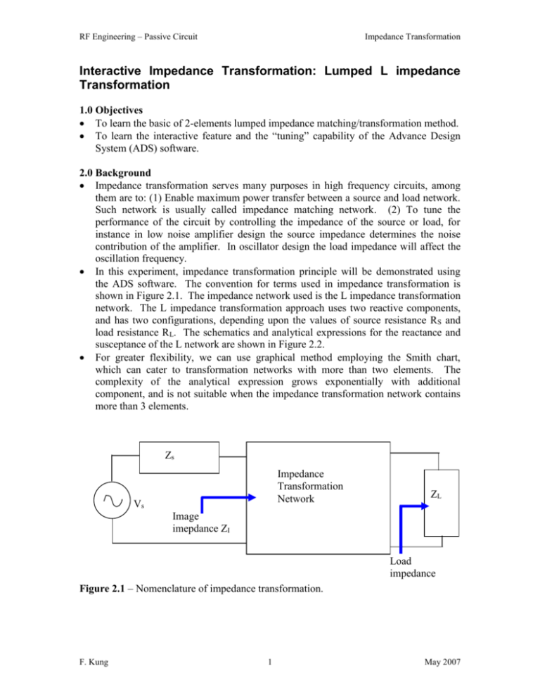
RF Engineering – Passive Circuit Impedance Transformation Interactive Impedance Transformation: Lumped L impedance Transformation 1.0 Objectives To learn the basic of 2-elements lumped impedance matching/transformation method. To learn the interactive feature and the “tuning” capability of the Advance Design System (ADS) software. 2.0 Background Impedance transformation serves many purposes in high frequency circuits, among them are to: (1) Enable maximum power transfer between a source and load network. Such network is usually called impedance matching network. (2) To tune the performance of the circuit by controlling the impedance of the source or load, for instance in low noise amplifier design the source impedance determines the noise contribution of the amplifier. In oscillator design the load impedance will affect the oscillation frequency. In this experiment, impedance transformation principle will be demonstrated using the ADS software. The convention for terms used in impedance transformation is shown in Figure 2.1. The impedance network used is the L impedance transformation network. The L impedance transformation approach uses two reactive components, and has two configurations, depending upon the values of source resistance RS and load resistance RL. The schematics and analytical expressions for the reactance and susceptance of the L network are shown in Figure 2.2. For greater flexibility, we can use graphical method employing the Smith chart, which can cater to transformation networks with more than two elements. The complexity of the analytical expression grows exponentially with additional component, and is not suitable when the impedance transformation network contains more than 3 elements. Zs Impedance Transformation Network Vs ZL Image imepdance ZI Load impedance Figure 2.1 – Nomenclature of impedance transformation. F. Kung 1 May 2007 RF Engineering – Passive Circuit Impedance Transformation jX jB ZI = Rs + jXs RL + jXL (a) For RL>Rs RL + jXL (b) For RL<Rs jX jB ZI = Rs + jXs Figure 2.2 – The two configurations for L impedance transformation network. For RL<RS: B RS RL RL X S RS 2 RS X S X 2 R SR L S 2 X BRS RL X S XL 1 BX S For RL>RS: B XL R L X L RS R L 2 RL RS RL X L 2 2 2 X R 1 X L RS S XS B RL RL B 3.0 Introduction to the Experiment In this example we want to transform a complex load impedance to ZI = 35+j20 at 450.0 MHz. The load is modeled by a 300 resistor in parallel with a 0.82 pF capacitor. At 450.0 MHz, the load impedance ZL can be calculated as: Z L R // j1C R 1 jRC 2 450 10 6 Z L 202 .1852 j140 .6297 Since Re Z L RL 202 .1852 Re Z s Rs 35 , configuration (a) of Figure 2.2 is used. 4.0 The Experiment Procedures 1. Log into workstation. F. Kung 2 May 2007 RF Engineering – Passive Circuit Impedance Transformation 2. Run the ADS version 2003A software (you might use a newer version of the software). 3. From the main window of ADS, create a new project folder named “Impedance_Transform” under the directory “D:\ads_user\default\” (Figure 4.1). Figure 4.1 – Opening a new project in ADS. 4. The new schematic window will automatically appear once the project is properly created. Otherwise you can manually create a new schematic window by double clicking the Create New schematic button on the menu bar. 5. Draw the schematic as shown in Figure 4.2. In using configuration (a) of Figure 2.2, we assume that the susceptance B can be synthesized by capacitor C 1 while the reactance X can be synthesized by inductance L1. Initially set C1 = 0 and L1 = 0. Save the schematic as “schematic1.dsn”. The various components used in Figure 4.2 can be obtained from the palette list of the draw schematic window as shown in Figure 4.3. We see from Figure 4.2 that this is an S-parameter simulation, requesting the software to calculate the S-parameters as seen from component Term1 at frequency 450 MHz. In this case the parameter Step in the S-parameter simulation control is ignored. F. Kung 3 May 2007 RF Engineering – Passive Circuit Impedance Transformation We wish to find s11 as seen from Term1 Figure 4.2 – The schematic. Figure 4.3 – The pallete for lumped components. 6. Now run the simulation by clicking the button F. Kung 4 . May 2007 RF Engineering – Passive Circuit Impedance Transformation 7. The ADS software will automatically invoke a data display window. The data display window is used to show the result of the simulation. You can also invoke the data display window manually by clicking the button . 8. Insert a Smith Chart in the data display window as shown in Figure 4.4. Click this button to insert an X-Y plot Click this button to insert a Smith chart Display area Click this button to insert an equation in the display area Select S(1,1) to show the s11 as measured from Term1 in the Smith chart Figure 4.4 – Inserting a Smith chart in the display area. Also shown are typically used buttons. F. Kung 5 May 2007 RF Engineering – Passive Circuit Impedance Transformation 9. You can change the color, the thickness of the line and the format of the Smith chart by using the Trace Option and Plot Options tab as shown in Figure 4.5. Figure 4.5 – Changing the properties of a plot. Enabling both impedance and admittance coordinates in the Smith chart. Hints: To show both impedance and admittance lines on the Smith chart, double click on the chart and modified the plot options, select “both” for the coordinate. 10. Your Smith Chart should look similar to the one shown in Figure 4.6. Use a Marker to display the complex value of the s11. Note that both impedance and admittance coordinates are shown in the Smith Chart (See Figure 4.5 again if you do not know how to set this). F. Kung 6 May 2007 RF Engineering – Passive Circuit Impedance Transformation Marker The value of S11 and impedance as indicated by the Marker Position of S11 in the Smith chart Figure 4.6 – The Smith chart for s11 at 450 MHz as seen from component Term1. 11. Now we also want to show the s11 of the required image impedance ZI on the Smith chart. This can be done by first calculating the s11 of ZI = 35+j20 using equations inserted into the data display area. The equations are shown in Figure 4.7. Note that s11 = I , the reflection coefficient of the impedance. Figure 4.7 – The equations for finding s11 of the image impedance ZI (Note that we use ZS = ZI in this case). 12. Now insert s11 for ZI as shown in Figure 4.8a. The resultant Smith Chart should be as shown in Figure 4.8b. At this stage you should save the data display, save it as “schematic1.dds”. F. Kung 7 May 2007 RF Engineering – Passive Circuit Impedance Transformation Figure 4.8a – Selecting the result of equations. Impedance transformation Due to L1 Due to C1 Figure 4.8b – The final Smith Chart, with the effect of adding C1 and L1 illustrated. 13. The function of the L impedance transformation is to transform ZL = 202.1852j140.6297 into ZI = 35 + j20 at 450 MHz. This is accomplished through the effect of adding a susceptance (as created by C1) and a reactance (as created by L1). Using a graphical method such as Smith Chart allows us to visualize the effect of C1 and L1. These elements modify the position of Marker m1, until it gradually reaches the position of Marker m2, as illustrated in Figure 4.8b. The position of m2 corresponds F. Kung 8 May 2007 RF Engineering – Passive Circuit Impedance Transformation to ZI = 35 + j20 (at 450 MHz). When we achieved this, the impedance transformation network design will be done. 14. The ADS software has a powerful tuning feature, which allows us to change the value of the components in the circuit while it updates the results in real-time. A typical simulation process in ADS needs a large amount of pre-processing before the actual calculation is carried out. The pre-processing involves setting up the appropriate variables and the memory of the computer based on the schematic and simulation control. During the “tuning” process, the ADS assumes the setup of the schematic and simulation to be unchanged, therefore the pre-processing is carried out once and calculation is run whenever the parameter-under-tuned is changed. This capability is useful for interactive design such as impedance transformation using the graphical method. 15. Enable the “tuning” mode by pressing the following pushbutton in the standard toolbar . 16. Use the mouse cursor to select the parameter of L1 and C1 in the schematic window, press Details button and set the step size and max step value as shown in Figure 4.9. The software will automatically rerun the simulation after each change is detected on value L1. Also set Trace History to 0 or 1. Now adjust the sliders control for L1 and C1 until the marker m1 moves to m2 in the Smith chart. You should adjust the slider for C1 and then follow by L1 (can you figure out why?). The final Smith Chart is shown in Figure 4.10. After you are satisfied with the result, press the Update button to permanently change the values of L1 and C1 in the schematic window. Figure 4.9 – The tuning dialog box. F. Kung 9 May 2007 RF Engineering – Passive Circuit Impedance Transformation Figure 4.10 – After tuning the values of L1 and C1, both Markers m1 and m2 overlap on each other, signifying the impedance transformation is done. 17. The final schematic is as shown in Figure 4.11. Modify the S-parameters simulation control as shown, with the start frequency at 200 MHz and the stop frequency at 1000 MHz. Also enable the calculation of Z-parameters from the S-parameters by double clicking the S-parameters simulation control and setting the check box as depicted in Figure 4.12. Now save this schematic as “schematic2.dsn”. Figure 4.11 – The final schematic. F. Kung 10 May 2007 RF Engineering – Passive Circuit Impedance Transformation Figure 4.12 - Enabling the Z-parameters calculation. 18. Now run the simulation again, after which the software will invoke a second data display window for “schematic2.dsn”. This time instead of plotting the s11 as seen by Term1 in a Smith chart, plot the z11 as seen by Term1 as two X-Y plots, one showing the real part and the other showing the imaginary part versus frequency. The result is as shown in Figure 4.13. Using the markers, it is verified that we obtained the required impedance at 450 MHz. Note that z11 = ZI in this one-port network. F. Kung 11 May 2007 RF Engineering – Passive Circuit Impedance Transformation Figure 4.13 – X-Y plots of real and imaginary parts of ZI. 19. A final note, by now you would notice that the impedance transforming network only works at one frequency, i.e. 450 MHz for this example. This is true for all impedance transformation networks. However you would notice that within a small range of frequency centered at 450 MHz, known as the bandwidth, the impedance transformation network still works reasonably well, i.e. the parallel RC load network still tranformed to 35+j20 approximately. For the L networks, we cannot control the operating frequency range, but for higher order networks such as T, pi or ladder networks, one can control the bandwidth for a constant load impedance. Refer to the lecture notes for more details on the bandwidth. 20. Extra procedure – Use the analytical formulae for B and X of Figure 2.2 to derive the exact values for L1 and C1. Compare these with the values obtained using interactive approach in ADS software. NOTE No report is needed for this experiment. You would be evaluated on-the-spot during the experiment. F. Kung 12 May 2007
