Assignments - Guru Tegh Bahadur Institute of Technology
advertisement

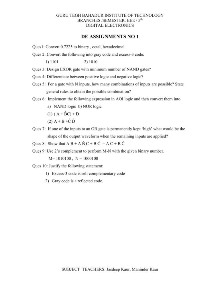
GURU TEGH BAHADUR INSTITUTE OF TECHNOLOGY BRANCHES /SEMESTER: EEE / 5th DIGITAL ELECTRONICS DE ASSIGNMENTS NO 1 Ques1: Convert 0.7225 to binary , octal, hexadecimal. Ques 2: Convert the following into gray code and excess-3 code: 1) 1101 2) 1010 Ques 3: Design EXOR gate with minimum number of NAND gates? Ques 4: Differentiate between positive logic and negative logic? Ques 5: For a gate with N inputs, how many combinations of inputs are possible? State general rules to obtain the possible combination? Ques 6: Implement the following expression in AOI logic and then convert them into a) NAND logic b) NOR logic (1) ( A + B́C) + D (2) A + B +C̀ D́ Ques 7: If one of the inputs to an OR gate is permanently kept ‘high’ what would be the shape of the output waveform when the remaining inputs are applied? Ques 8: Show that A B + A B́ C + B Ć = A C + B Ć Ques 9: Use 2’s complement to perform M-N with the given binary number. M= 1010100 , N = 1000100 Ques 10: Justify the following statement: 1) Excess-3 code is self complementary code 2) Gray code is a reflected code. SUBJECT TEACHERS: Jasdeep Kaur, Maninder Kaur GURU TEGH BAHADUR INSTITUTE OF TECHNOLOGY BRANCHES /SEMESTER: EEE / 5th DIGITAL ELECTRONICS DE ASSIGNMENTS NO 2 Ques 1: Find the values of the two valued variables A , B , C and D by solving the set of simultaneous equations : Ā+AB=0 AB = AC AB+AČ+CD=Č D Ques 2: Simplify logic function using Q – M minimization technique Y( A , B , C, D) = ∑ m ( 0, 1, 3, 7, 8, 9,11,15) Ques 3: Simplify the Boolean expression using four variables: w’ z + x z + x’ y + w x’ z Ques 4: Simpify the following Boolean expression using Don’t Care in a) SOP form b) POS form (1) F( A , B , C, D) = ∑ ( 0 , 6, 8 , 13, 14) (2) d ( A, B, C ,D) = ∑ ( 2 , 4, 10 ) Ques 5: Simpify the boolean expression: a) F(A, B ,C, D) = Π (1, 5,4, 7, 12, 14) b) F(A, B ,C, D) = Π (0, 2, 3,8 ) Ques 6: Find the minimum POS and SOP expression for the function using K-maps. F(A,B,C,D) =∏ M(0, 2, 6, 8, 9, 10) + D( 5, 12,13,14,15) where D donotes Don’t care terms. SUBJECT TEACHERS: Jasdeep Kaur, Maninder Kaur GURU TEGH BAHADUR INSTITUTE OF TECHNOLOGY BRANCHES /SEMESTER: EEE / 5th DIGITAL ELECTRONICS DE ASSIGNMENTS NO 3 Ques 1: Design FULL ADDER using two HALF ADDER? Write its truth table also? Ques 2: Design FULL SUBRATOR using two HALF SUBTRATOR? Write its truth table also? Ques 3: Design a combinational circuit with three inputs X, Y and Z & three outputs A, B and C. When the binary input is 0, 1, 2 or 3, the binary outputs is one greater than the input. When the binary input is 4, 5, 6 or 7, the binary output is one less than input? Ques 4:You are presented with a set of requirements under which an insurance policy can be issued. The applicant must be: 1) 2) 3) 4) 5) a married female 25 years old or over , or a female under 25 , or a married male under 25 who has not been involved in a car accident , or a married male under 25 who has been involved in a car accident, or a married male 25 year or over who has not been involved in a car accident. Find an algebraic expression which assumes a value 1 whenever the policy is issued. Simplify the expression obtained. Ques 5: In an application 4 inputs A, B, C, D are available in true and complement Form .These are fed at a logic circuit which operates a relay. The relay is ON for ABCD = 0000, 0010, 0101, 0110, 1101 and 1110. The states 1000 and 1001 don’t occur. For remaining states the relay is OFF. a) prepare truth table and minimize outputs F using K map b) Realize F using 3 input NAND gates. Ques 6: Design a combinational circuit that produces the binary sum of two 2-bit number X1, X2 and Y1, Y2. Ques 7: Describe the operation of look-ahead carry adder .What are its advantages over ordinary adder? SUBJECT TEACHERS: Jasdeep Kaur, Maninder Kaur GURU TEGH BAHADUR INSTITUTE OF TECHNOLOGY BRANCHES /SEMESTER: EEE / 5th DIGITAL ELECTRONICS DE ASSIGNMENTS NO 4 Ques 1: A circuit receives a 4- bit excess -3 code. Design a minimal circuit to detect the decimal number 0, 1 ,4, 7 and 8? Ques 2: Design and implement 4- bit gray to binary converter? Ques 3: Design and implement SOP circuit that will generate an odd parity bit for a 4bit input? Ques 4: Design 4- bit magnitude comparator? What is the function of cascading inputs in magnitude comparator? How are they connected? Ques 5: A one bit full adder is to be implemented using 8:1 MUX a) Write truth table for SUM(S) and Carry (C) in terms of two bits A and B and carry from previous stage. b) Implement S and c using 8:1 MUX. Ques 6: Design 16: 1 MUX using only 4: 1 MUX? Ques 7: Implement full subtractor using Decoder? Ques 8: Implement the expression using multiplexer: (1) F( A , B , C, D) = ∑m( 0 , 2, 3,6, 8 , 13, 14) SUBJECT TEACHERS: Jasdeep Kaur, Maninder Kaur GURU TEGH BAHADUR INSTITUTE OF TECHNOLOGY BRANCHES /SEMESTER: EEE / 5th DIGITAL ELECTRONICS DE ASSIGNMENTS NO 5 Ques 1: Differentiate between: a) Multiplexer and demultiplexer b) Encoder and decoder c) Decoder and demultiplexer d) PLA and PAL Ques 2: What is the function of select lines in demultiplexer? Ques 3: Implement the following minterm expression using decoder: (2) F1= ∑ ( 0 , 6, 8 , 13, 14) (3) F2= ∑ 5, 7 ,9 11, 15) (4) F3= ∑ ( 0 , 4, 5) (5) F4= ∑ ( 12, 13 ,15) Ques 4: Convert BCD code to Excess-3 code and implement it using PLA? Ques 5: Implement Full adder using PLA? Ques 6: Implement the following Boolean function with PAL: 1) w(A,B,C,D)= ∑ ( 2, 12,13) (6) x(A,B,C,D)= ∑ (7,8,9,10,11,12,13,14,15) (7) y(A,B,C,D)= = ∑ ( 0 ,2,3, 4, 5,6,7,8,10,11,15) (8) z(A,B,C,D)= = ∑ ( 1,2,8,12,13) SUBJECT TEACHERS: Jasdeep Kaur, Maninder Kaur GURU TEGH BAHADUR INSTITUTE OF TECHNOLOGY BRANCHES /SEMESTER: EEE / 5th DIGITAL ELECTRONICS DE ASSIGNMENTS NO 6 Ques 1: A JN flip flop has two inputs J and N .Input J behaves like the J input of a JK flip Flop and Input N behaves likes the complement of the K input of JK flip flop (N = K’) a) Tabulate the Characteristic table of the flip flop b) Tabulate the excitation table of the flip flop c) Convert it into D flip flop Ques 2: What is Race problem in flip flop? How it it is overcome? Ques 3: How can the initial state of a flop flop be fixed using preset and clear terminals. Ques 4: Deswign an synchronous up/down counter with four states (0,1,2,3) using clocked JK flip flop . a control signal (X) is to be used as follows When x = 0, the circuit counts forward( up) When x = 1, the circuit counts backward( down) Ques 5: Design a master slave flip flop using 9 Nand gate. Ques 6: Connect a D flip flop in such a manner that it will perform like cloked T flip flop Ques 7: Construct a D flip flop using only JK Flip flop and no additional gates. SUBJECT TEACHERS: Jasdeep Kaur, Maninder Kaur GURU TEGH BAHADUR INSTITUTE OF TECHNOLOGY BRANCHES /SEMESTER: EEE / 5th DIGITAL ELECTRONICS DE ASSIGNMENTS NO 7 Ques 1: Explain the difference between the Mealy model and Moore model (with sequence state diagram ) for a sequential circuit for an input sequence of x = 011010 Ques 2: Design a synchronous sequential circuit with one input x and output z that Recognize the input sequences 01 .Show the state diagram and state table for the circuit designed. Ques 3: What are the differences between state diagram and state table? Ques 4: Draw the state diagram sate table and excitation table of an sequence detector that produces an output 1 when ever the non over lapping sequence 1011 is detected? Ques 5: Compare Synchronous and asynchronous Sequence logic circuits? SUBJECT TEACHERS: Jasdeep Kaur, Maninder Kaur GURU TEGH BAHADUR INSTITUTE OF TECHNOLOGY BRANCHES /SEMESTER: EEE / 5th DIGITAL ELECTRONICS SUBJECT TEACHERS: Jasdeep Kaur, Maninder Kaur


