Surface Resistivity and Static Decay
Federal Test Standard 101C, Method 4046.1 requires a static protective material to have a static decay time
of less than 2 seconds. EIA 541 defines a static dissipative material as one, which has a surface resistivity of
between 1E5 and 1E12 Ohms per square. These two requirements are correlatable only for monolayer and
homogeneous films. Multi-layer coextrusion technology as well as laminated materials separate these two
parameters. Note: the term 1E5 is a short version of 1X10⁵.
Although many experts have discussed this fact in regards to laminated metallized materials, the conception
persists that a low surface resistivity is required to dissipate a static charge and that a good static decay is
sufficient to characterize a dissipative material. The dissipation of static charges may be accomplished by
several means: across the surface, by volumetric conduction through a relatively thin high resistivity skin, across
a subcutaneous conductive or dissipative layer and out of the film again through the thin high resistivity skin.
HOMOGENEOUS MATERIALS
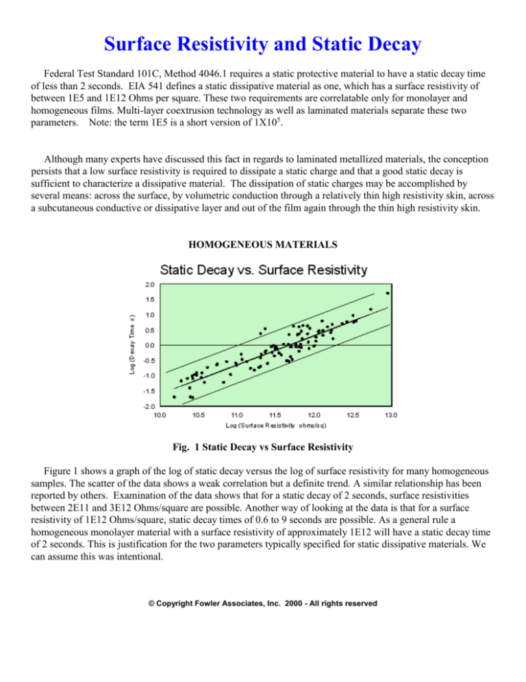
Fig. 1 Static Decay vs Surface Resistivity
Figure 1 shows a graph of the log of static decay versus the log of surface resistivity for many homogeneous
samples. The scatter of the data shows a weak correlation but a definite trend. A similar relationship has been
reported by others. Examination of the data shows that for a static decay of 2 seconds, surface resistivities
between 2E11 and 3E12 Ohms/square are possible. Another way of looking at the data is that for a surface
resistivity of 1E12 Ohms/square, static decay times of 0.6 to 9 seconds are possible. As a general rule a
homogeneous monolayer material with a surface resistivity of approximately 1E12 will have a static decay time
of 2 seconds. This is justification for the two parameters typically specified for static dissipative materials. We
can assume this was intentional.
© Copyright Fowler Associates, Inc. 2000 - All rights reserved
METAL LAMINATES
Fig. 2 Metal In Shielding Material
Figure 2 shows a "metal in" laminated shielding material. This material has a dissipative low-density
polythylene layer on one side and a 48-gauge polyester terephthalate (PET) layer on the other. The metallized
side of the PET is adhesive laminated to the polyethylene. The surface resistivity of the polyethylene side may
be approximately 1E11 Ohms/Square. The PET side is >1E14 Ohms/square. However the static decay is < 10
milliseconds regardless of which side is viewed during the static decay test.
Figure 3 illustrates a "metal out" shielding material. It has a dissipative poly layer on one side and a
protective coating over a metallization layer on the other. The surface resistivity of both sides of the material
may be below 1E12 Ohms/square. Again the static decay is < 10 milliseconds regardless of the side viewed
during the test.
Fig. 3 Metal Out Shielding Material
The reason for the seemingly fast dissipation of charges is that the static decay time is dominated by voltage
suppression or, more correctly, by the near instantaneous decay of induced charges on the metal layer. In Figure
4 the sensor detects this induced charge only while the high voltage is applied to the outer layers of the material.
As soon as the high voltage is removed and ground is connected to the electrodes, the polarized charge is
relaxed very quickly giving the appearance of rapid decay of surface charges. The voltage resulting from any
charges remaining on the surface of the non metal layer is suppressed by the ground plane being capacitively
coupled to the metal layer. Therefore, for laminated materials with buried metal layers, the decay times
measured in the Method 4046.1 test fixture are not related to surface resistivity.
Fig. 4 Induced Charges on Metal Layer In Shielding Material
For metal laminates with surface resistivities less than 1E12 Ohms/square, one can assume that the surface
charges decay in less than 2 seconds. For those layers with resistivities above this level, no assumption can be
made from the results of the static decay test as described in Method 4046.1 .
MULTI-PLY COEXTRUDED MATERIAL
The application of laminations or coextrusion technology to ESD materials allows the separation of the
parameters of surface resistivity and static decay for laminates that do not contain metal or metallized layers.
Coextrusion is the process of forming multi-layer materials from several extruders directly out of a one special
die. This is different from laminations where individual layers of film are glued or extrusion coated together to
form a multi-layer material. In coextrusion processes, very thin layers of various materials can be formed
continuously. Each layer may be designed for particular physical, chemical, or electrical properties. Figure 5 is a
cross section of a five layer coextruded ESD packaging material. This example has no metallization layer.
Fig. 5 Coextruded Film
In a coextruded material, each layer can be made from different base polymers or a blend of polymers, each
selected for design attributes such as moisture barrier, flame retardancy, sealability, stiffness or strength. Where
ESD protective properties are desired, one or all layers can be compounded with anti-static additives. The
loading levels, polymer and additive types can be varied for desired effects.
The outside layers may be designed for anti-static (non tribo charging), dissipative, or non-contaminating
attributes. The internal layers can add barrier, strength, dissipation or other properties. If all layers have
dissipative properties, the material will exhibit some level of volume conductivity.
The total thickness of the structure is 3 mils. The individual thicknesses may be varied greatly. However, an
outer layer of only a small fraction of a mil is achievable. If the internal layers are made dissipative by anti-static
additives and the external layers are left as pure polymers, the total structure will exhibit reasonable static
dissipative properties without the required < 1E12 Ohms/square surface resistivity. During the coextrusion
process, the additives can penetrate a short distance into the outer layer causing a gradient of conductivity as
viewed from the outside. However the external surfaces remain clean (free of contaminates such as anti-static
agents or lubricants). Materials such as this may also be constructed using lamination techniques.
Figure 6 shows a graph of the log of static decay versus the log of surface resistivity for multi-ply materials.
For materials with surface resistivities less than about 5E11 Ohms/square, the static decay follows the same
trend as that shown in Figure 1 for homogeneous materials. This is because the coextruded material has
dissipative skins. However, for materials with surface resistivities above 5E11 Ohms/square, and dissipative
inner layers, the static decay times become dependent on the resistivity of the inner layers.
Fig. 6 Static Decay vs Surface Resistivity For Multi-Ply Materials
If the external as well as internal layers are compounded with anti-static/dissipative properties, the total
structure will exhibit all normal relationships of conductivity, static decay and anti-staticity. However, as with
monolayer materials, the cleanliness of a totally loaded structure is somewhat less than that of its clean or
"neutral skin" counterpart.
Multi-ply materials allow an ESD protective packaging user to weigh the individual benefits of all material
attributes without them being totally dependent on one another. Surface resistivity measurements assume that a
material is homogeneous. When a material is a laminate or a coextrusion the concept of surface resistivity is
invalid. The volume contribution of the resistance becomes important in the determination of the ability of a
material to conduct charges. When a multi-ply material has clean skins and a gradient of anti-static additives in
the bulk of the structure, its actual ability to dissipate charges is related to many factors. Resistance of the
surface of the outer layers, bulk or volume resistance of the individual layers, voltage gradient of the
measurement electrode configuration and, for rapid discharges, polarity of the composite materials all play an
important part in the dissipation of charges.
Surface resistivity measurements poorly estimate the total effects of the parameters. This is not to say that a
material with a surface resistivity of < 1E12 Ohms/square does not dissipate charges. On the contrary, if the
surface resistivity is within the limits specified by the EIA, charges will be dissipated and the static decay
numbers will probably be within specifications. However, if a material has a higher than 1E12 Ohms/square
surface resistivity, it may not accumulate charges but rather dissipate them through the mechanisms just stated.
Its static decay may also be within specifications due to charge dissipation. The static decay of a multi-ply
material with a dissipative layer below the surface may also have a rapid static decay time related to relaxation
of induced charges through the resistance of the internal layers just as described for metallized laminates.
Figure 7 shows a close up view of one surface resistivity measurement of a 3-mil multi-ply material. In this
view, the relative dimensions are obvious. While the electrode separation is only 1/32 of an inch, the layer
thicknesses are much less. If the outer layers have a relatively high resistance and the inner layers are more
conductive, the ability to dissipate charges is related to volume as well as surface conduction. If dipole motion is
considered for fast discharges, the total dissipative ability is more clear.
Fig. 7 Cross Section of Surface Resistivity Measurement
In the ASTM D-257 surface resistivity measurements, the voltages used are not standardized. There is also no
standardization of electrode configuration. Therefore the voltage gradient is a large variable to the determination
of a material's impedance to charge dissipation. Measurements are made with voltages ranging from 10 volts to
over 1000 volts. The following chart describes the variation in voltage gradients encountered in surface
resistivity measurements using annular electrodes.
VOLTAGE
ELECTRODE SEPARATION
VOLTAGE GRADIENT
10V
100V
500V
1/32 ”
1/32 ”
1/32 ”
320 V/inch
3200 V/inch
16000 V/inch
10 V
100V
500V
1000V
1/2 ”
1/2 ”
1/2 ”
1/2 ”
20 V/inch
200 V/inch
1000 V/inch
2000 V/inch
10V
100V
500V
1000V
3/4"
3/4"
3/4"
3/4"
13 V/inch
133 V/inch
666 V/inch
1333 V/inch
This indicates why ESD Association's S11.11 now fixes the electrode configuration as well as voltage
applied.
As in the measurement of surface resistivity, the real world mechanism of charge dissipation is dependent on
voltage gradient. Figure 8 illustrates the principle of voltage gradient from a charged conductor. If a conductor
shaped like the one in Figure 8 is charged, the charge density, or quantity of charge per unit area, is greatest at
the point of greatest curvature. The intensity of the electric field near the conductor is correspondingly greatest
near the point of greatest curvature.
The field intensity of the sharply curved point may be great enough to cause the medium surrounding the
point to become ionized and to produce corona discharges. The measurement of surface resistivity does not
approximate the actual discharge or dissipation of charges by a material. A person's finger or a sharp tool causes
very high voltage gradients even for relatively low charges. This allows more charge removal per unit time than
can be accurately predicted by surface resistivity measurements alone.
Fig. 8 Irregular Shaped Charged Conductor
During static decay tests and actual discharges from or to a material, the voltage gradient of the discharge
configuration, the dipole moment of the material and the combined resistance of the bulk of the material all play
a part in the ability of the material to dissipate or not retain charges.
Static events are not purely dc phenomena. They are a complex combination of ac, dc, neutralization and rf
mechanisms. Therefore surface resistivity measurements, being dc in nature, cannot correlate to decay or
dissipation in all situations.
There are three parameters by which a material may be deemed static safe: Charge generation, dissipation,
and retention.
Charge dissipation as just discussed is a material's ability to rid itself of most of the charge accumulated on
itself or from charged objects brought in contact with its surface.
CHARGE RETENTION
Charge retention is the amount of charge left on a charged object after it has been grounded for a certain
amount of time. The charge may be measured by a Faraday cup and electrometer or indirectly by a field meter.
Three different situations for determining retained charge are demonstrated in Figures 9, 10, and 11.
Fig. 9 Charge Retained on a Material after Being Placed on a Grounded Plane
Figure 9 shows that if a material is charged to some level Q, then placed on a grounded plane, it will conduct
or dissipate the charge to some lower level Q'. The actual amount of residual charge is dependent on, among
other factors, the original charge, voltage gradient to ground (Q = CV), and combined resistance to ground.
To measure the retained charge in Figure 9, the material is isolated from ground, then charged by electrode
contact or tribo charging to a specified level. The material is placed on the grounded plane for a predetermined
amount of time. It is then lifted off the plane and its charge or voltage is again measured. This is the retained or
residual charge.
Fig. 10 Charged Conductive Block Placed on a Grounded Material
In figure 10, a charged conductive block is placed on a grounded material. Again, the residual charge is
dependent on the same parameters as above plus the geometry of the charged block. If the block has sharp
edges, its charge density and, therefore, its voltage gradient will be relatively high. This will allow more charge
dissipation than predicted by the material's surface resistivity.
For Figure 11, the charged block must be isolated from ground by an insulating string. It is charged and then
placed on the grounded material for a predetermined amount of time. The block is then lifted and the residual
charge or voltage is measured.
Fig. 11 Charged Material Discharged by Touching with a grounded Finger
In both cases, for volume conductive or volume dissipative materials, the retained charge is nearly zero.
However, coextruded materials with relatively high surface resistivity can dissipate much of the charge without
the contamination concerns associated with bulk loaded anti-static agents.
If a charged material is discharged by touching it with a grounded finger as in Figure 11, the residual charge
is dependent on the same variables as before. In this case, if the material is some distance from ground, its
capacitance to ground is much smaller than in Figures 9 and 10. This means the voltage gradient due to the total
charge is greater. Therefore the ability to dissipate the charge is greater for a given material structure and
combined resistance. The charges will flow from the material until the driving forces and impedance's equalize.
The material in Figure 11 must be isolated from ground as it is charged. After charging to a specified level,
the material is touched by a grounded finger for a predetermined amount of time. The charge or voltage on the
material is then measured to determine the retained charge.
Again, for conductive or dissipative materials, the residual charge is essentially zero. For coextruded
materials with relatively high surface resistivities, the residual charge can be very low.
DISSIPATION THRESHOLD
The dissipation of most of the charges from or through a coextruded ESD packaging material is sensitive to
what can be phrased as a dissipation threshold. If the structure is totally compounded to allow volumetric as
well as surface conductivity for all or at least the outer layers, the material will exhibit a minimum dissipation
threshold. This means that Ohm's Law is straight forward. However, if the conductivity of the structure is a
gradient from the inside to the outside, the dissipation ability is dependent on the voltages or charge
concentrations involved. This means that for charge concentrations above a certain level, the material will
dissipate those charges down to an equilibrium level. Ohm's Law is more complicated in this situation.
Dissipation threshold is not a new concept. Most insulators exhibit this at higher levels of charge density.
When the charge density or voltage gradient on an insulator such as polytetrafluoroethylene reaches the
ionization potential of air or any medium in which it is immersed, the charge will for the most part avalanche off
the insulator. This is the insulator's threshold for the removal of the static charge. If a polymer has its threshold
modified by lamination or coextrusion and anti-static additive technology, this threshold may be designed to
exist at a more desirable level. Dissipation thresholds on the order of 50 volts are achievable.
If a 50 volt threshold is achievable with pure polymer surfaces, this means that a clean material can exhibit
reasonable static properties. A clean skin material may not meet all the specifications set by the EIA or the
Military. However, many applications need the reduction of additives present on the surface of materials and
can live with the slightly reduced electrical characteristics for the significantly increased physical benefits.
Users of ESD protective materials need to weigh the cost/benefit parameters in selecting appropriate
materials for specific applications. Probably no material can ever meet all the requirements of the ESD world.
It would be nice to have a heat sealable, transparent aluminum foil with a surface resistivity of 1E8
Ohms/square and a volume resistivity of 1E11 Ohms-cm and have an attenuation of at least 120 dB to all
electromagnetic frequencies. However, this material is a dream. It should be named
.
UNOBTAINIUM.
© Copyright Fowler Associates, Inc. 2000 - All rights reserved
