Observation of Large-Scale Features on Graphite
advertisement
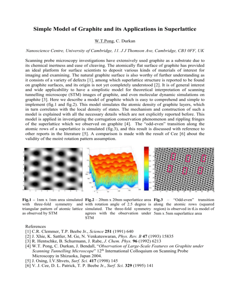
Simple Model of Graphite and its Applications in Superlattice W.T.Pong, C. Durkan Nanoscience Centre, University of Cambridge, 11. J J Thomson Ave, Cambridge, CB3 0FF, UK Scanning probe microscopy investigations have extensively used graphite as a substrate due to its chemical inertness and ease of cleaving. The atomically flat surface of graphite has provided an ideal platform for surface scientists to deposit various kinds of materials of interest for imaging and examining. The natural graphite surface is also worthy of further understanding as it consists of a variety of defects [1], among which superlattice structure is reported to be found on graphite surfaces, and its origin is not yet completely understood [2]. It is of general interest and wide applicability to have a simplistic model for theoretical interpretation of scanning tunnelling microscope (STM) images of graphite, and even molecular dynamic simulations on graphite [3]. Here we describe a model of graphite which is easy to comprehend and simple to implement (fig.1 and fig.2). This model simulates the atomic density of graphite layers, which in turn correlates with the local density of states. The mechanism and construction of such a model is explained with all the necessary details which are not explicitly reported before. This model is applied in investigating the corrugation conservation phenomenon and rippling fringes of the superlattice which we observed on graphite [4]. The “odd-even” transition along the atomic rows of a superlattice is simulated (fig.3), and this result is discussed with reference to other reports in the literature [5]. A comparison is made with the result of Cee [6] about the validity of the moiré rotation pattern assumption. Fig.1 – 1nm x 1nm area simulated with three-fold symmetry and triangular pattern of atomic lattice as observed by STM Fig.2 – 20nm x 20nm superlattice area with rotation angle of 2.5 degree is simulated. The three-fold symmetry agrees with the observation under STM Fig.3 – “Odd-even” transition along the atomic rows (squared region) is observed in this model of 5nm x 5nm superlattice area References [1] C.R. Clemmer, T.P. Beebe Jr., Science 251 (1991) 640 [2] J. Xhie, K. Sattler, M. Ge, N. Venkateswaran, Phys. Rev. B 47 (1993) 15835 [3] R. Hentschke, B. Schurmann, J. Rabe, J. Chem. Phys. 96 (1992) 6213 [4] W.T. Pong, C. Durkan, J. Bendall, “Observation of Large-Scale Features on Graphite under Scanning Tunnelling Microscope” 12th International Colloquium on Scanning Probe Microscopy in Shizuoka, Japan 2004. [5] J. Osing, I.V.Shvets, Surf. Sci. 417 (1998) 145 [6] V. J. Cee, D. L. Patrick, T. P. Beebe Jr., Surf. Sci. 329 (1995) 141
