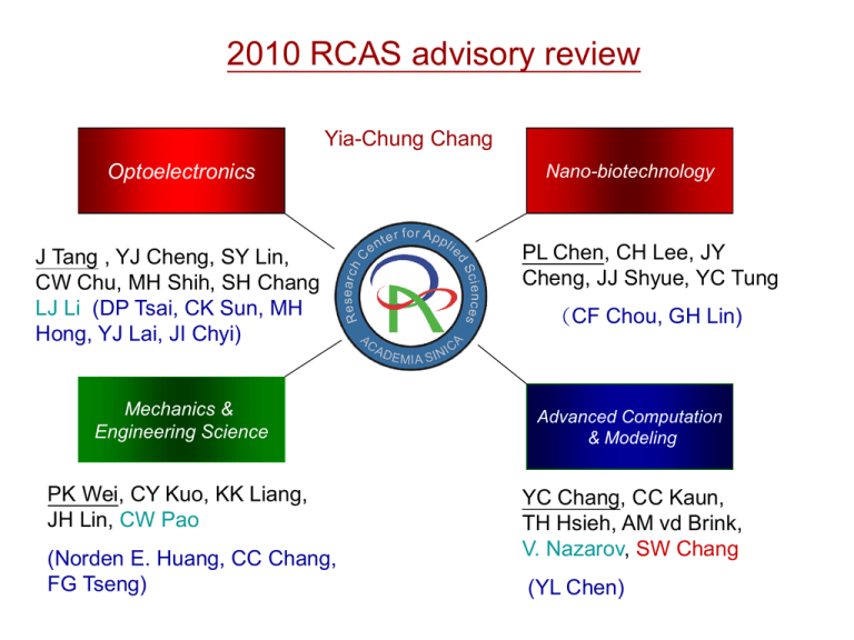
2010 RCAS advisory review
Yia-Chung Chang
Optoelectronics
J Tang , YJ Cheng, SY Lin,
CW Chu, MH Shih, SH Chang
LJ Li (DP Tsai, CK Sun, MH
Hong, YJ Lai, JI Chyi)
Nano-biotechnology
PL Chen, CH Lee, JY
Cheng, JJ Shyue, YC Tung
(CF Chou, GH Lin)
Mechanics &
Engineering Science
Advanced Computation
& Modeling
PK Wei, CY Kuo, KK Liang,
JH Lin, CW Pao
YC Chang, CC Kaun,
TH Hsieh, AM vd Brink,
V. Nazarov, SW Chang
(Norden E. Huang, CC Chang,
FG Tseng)
(YL Chen)
Advanced Computation& Modeling
張亞中 (YiaChung Chang) –
Nanostructure
electronics &
photonics
馬尚德 (Alec Maassen
van den Brink)–
Quantum computing
謝東翰(Tung-Han
Hsieh) – Web computing
New Hire: Shu-Wei Chang
關肇正 (Chao-Cheng
Kaun)– Ab initio transport
Vladimir Nazarov-CDFT
-Nanophotonics
Thematic Center for Optoelectronics
Yuh-Jen
Cheng
(程育人)
Jau Tang
(湯朝暉)
Shih-Yen Lin
(林時彥)
Chih-Wei Chu
(朱治偉)
Ming-Hsiung Shih
(施閔雄)
Lain-Jong Li
(李連忠)
Shih-Hsin Chang
(張仕欣)
Thematic Center for
Mechanics and Engineering Science
Chih-Yu Kuo
(郭志禹)
Pei-Kuen Wei
(魏培坤)
Kuo-Kang Liang
(梁國淦)
Chun-Wei Pao
(包淳偉)
Jung-Hsin Lin
(林榮信)
Nano-biotechnology(奈米生物組)
Chau-Hwang Lee
(李超煌)
Jing-Jong Shyue
(薛景中)
Ji-Yen Cheng (鄭郅言)
Peilin Chen (陳培菱 )
Yi-Chung Tung (董奕鍾)
Significant events
Personnel:
•
•
•
•
•
•
•
•
•
Dr. Chih-Wei Chu (朱治偉) has been promoted to associate research
fellow, effective January 8, 2010.
Dr. Pei-lin Chen (陳培菱) has been promoted to research fellow, effective
March 10, 2010.
Dr. Chao-Hwang Lee (李超煌) has been promoted to research fellow,
effective May, 2010.
Dr. Chun-Wei Pao(包淳偉) was appointed as assistant research fellow,
starting November 1, 2009.
Dr. Lain-Jong Li (李連忠) was appointed as associate research fellow,
starting Februay 1, 2010.
Dr. Vladmir Nazarov was appointed as associate research fellow, starting
on July 1, 2010.
Dr. Shuwei Chang (張書維) (Ph.D, University of Illinois, UrbanaChampaign) is expected to report to work as assistant research fellow in
September, 2010.
Dr. Pei-lin Chen (陳培菱) was appointed as the associate director for
general affairs, starting June 15, 2010
Three candidates (V. Podzorov, Chao-Min Cheng, and E. Il'ichev) were
interviewed, and two female candidates have been scheduled to have an
interview in August. Decision will be made after August to select one or
two candidates.
Outreach & Activities
–
–
–
–
–
–
–
–
RCAS organized a RCAS Taiwan-Japan Workshop on Single
Molecule/Confocal Microscopy during on Oct. 15, 2009. A delegation from
National Institute of Advanced Industrial Science and Technology (AIST),
Japan was invited to attend the workshop.
RCAS co-sponsored the 6th ACUP (Asian Conference on Ultrafas Phenomena)
held at NTU during Jan. 10-13, 2010.
RCAS invited Dr. Monique Combescot (Director of 1st Class, CNRS, Paris) to
give a lecture series on “Many-body theory of Exciton Condensation” in
Academia Sinica during January 11-22, 2010.
The second annual RCAS workshop has been held on Feb. 10 and 11, 2010.
In the workshop, Total attendance was around 200.
RCAS and NCTU arranged a NCTU-RCAS Optoelectronics Workshop on
March 5, 2010 to exchange research experience and discuss future
collaborations. RCAS Optoelectronics group held an open house for all NCTU
students during the afternoon of that day. A follow-up collaboration proposal
wasestablished.
RCAS will co-organized the 2010 Cross-Strait Workshop on Engineering
Mechanics (海峽兩岸工程力學研討會) in May, 2010. The main organizer is
Institute of Applied Mechanics, National Taiwan University.
RCAS Invited Nobel laureate, Prof. Ahmed Zewail to visit AS during June
28&29,2010 and give a lecture.
RCAS established the ANNA(Asian Nanoscience & Nanotechnology
Association) – Taiwan Chapter (Jau Tang and L. J. Li served as Chair &
Executive Officer) Prof. Ahmed Zewail will serve as the honorary
President of ANNA.
Space
Current situation:
Nanobio group:
2F of IoP (~1000 m2)
B2F(~400 m2)
Headquater & ACM group:
11F(~400 m2) + 3 offices (~70 m2)
on 10F, Humanity & Social Science Building
4 offices in Institute of Ethnics (~100 m2)
Mechanics group: 17 offices (~500 m2) in Institute of
History and Linguistics
Optoelectronics group : 5F, Tien-Chia-Ping building and 5F,
Microelectronics and Information System Research Center ,
NCTU (~1600 m2)
Building plans
RCAS expects to have two branches:
• Taipei Branch- biotechnology related research
The administration staff, nano-bio group, mechanics group, and
part of the advanced computation group will be located in
the“Coordinated Science and Technology Building”on the Sinica
campus. (estimated area= 1500 pings = 5000m2)
• Hsin-chu Branch- semiconductor related research
It is proposed that the optoelectronics/advanced materials
group and part of the advanced computation group will be
located in a new building on the NCTU campus. Currently, there
are two options for the building site:
1. Between the Tien-Chia-Ping building and the 4th Engineering
Building(工四館) (estimated area= 1100 pings = 3600m2)
2. Near the south gate of NCTU,next to NSRRC, NTHU, and Industrial
Park. (estimated area= 1500 pings = 5000m2)
中央研究院跨領域科技研究大樓新建工程
委託單位:中央研究院
規劃設計:潘冀聯合建築師事務所
2009.6.30
方案一 田家炳增建透視圖
5
F
[
9
F
工
六
館
]
]
工
五
館
田
家
炳
光
電
中
心
[
[
6
F
]
]
]
F
工
四
館
6
F
[
7
工
三
館
]
7
F
工
三
館
[
4
F
科
學
一
館
[
[
田
家
炳
光
電
中
心
中
研
院
研
究
中
心
[
工
六
館
]
往北大門
8
F
]
5
F
[
交
映
樓
7
F
]
交
映
樓
[
]
6
F
視角一
田家炳光電中心東
側銜接
往南大門
視角二
方案一 標準層平面圖
田家炳光電大樓
4.8
4.9
建築面積=505㎡,地下一層、地上七層(1樓挑高)
地下一層面積=505㎡(地下停車場15輛)
一至七層面積=505x7=3535㎡
估計造價:主體結構8000萬元、裝修設備3500萬
2
總樓地板面積=3605㎡
11.8
中研院研究中心新建面積
共同實驗室
教師辦公室
教師辦公室
空調
機房
教師辦
公室
個人研究室
教師辦公室
教學準備室
交誼廳
教學準備室
應科大樓
7F
教師辦
公室
教師辦
梯廳 公室
個人研究室
個人研究室
7.4
教學實驗室
個人研究室
貴重儀器
實驗室
男廁
個人研究室
個人研究室
7.4
教學實驗室
個人研究室
教學實驗室
資訊.電氣室
女廁
女廁
儲藏室
7.4
NCTU 鑽石計畫頂尖研究中心大樓
一、基地位置:
基地位置:新南大門東側。
基地面積:約1.9公頃。
基地位置示意圖
一、基地現況
東北季風
東西晒
休閒區
基地位置
面積:19000 m2
安
廣場
新
同步輻射入口
新
安
路
新南大門
同步輻射研究中心
路
國家高速電腦中心
二、建築規劃:
建築面積約3,300 ㎡。
樓地板面積26,400 ㎡。
需求量
體
使用單位
中研院應科中心、原分
所
建築經費
經費來源
交大(電子、奈米、材
料、生醫、環境永續)
1,500坪 建築:約8億
結構體、室內
裝修、
6,500坪 空調設備。
合計
8,000坪
頂尖大學計畫經費
&中研院
約8億
依據上述使用空間計算所需留設之法定停車數量,作為地下室開挖面積概估。
RF
+4000
10F
+3600
9F
+3200
8F
+2800
7F
+2400
6F
+2000
2580 m2
5F
+1600
2580 m2
4F
+1200
2580
m2
3F
+800
2580 m2
2F
+400
2580 m2
1F
+0
2580 m2
B1
-350
1350 m2
1350m2
1350 m2
1350 m2
6000m2
同步輻射
10 m
四、方案設計
二、建築規劃
人群動線
服務動線
連結動線
廣場
方案 二
建築入口
陡坡
校園管制點
交大頂尖研究中心
1300m2×7(層)
綠帶
綠帶
1.可彈性設置建築入口的配置計畫,提供不同需求的
空間管制。
交大頂尖中心
1300m2×10(層)
中研院應科中心
1300m2×3(層)
2.H型的平面計畫,可平均分配基地中之開放空間。
3.建築錯落的配置,留設北向綠帶,強化與校區的連結。
4.水平向配置,與交大建築配置走向彼此呼應。
共用地下層
7200m2×1(層)
交大與中研院共同推動研究合作計畫草案
• 成立一經費委員會,專責處理經費。使用、分配、研究
推動及研究審查,成果報告及合作計劃擬定辦法修訂,
而委員會設置在交大光電中心之下運作。
• 經費委員會內設召集人一人,由委員會委員互相推舉產
生,委員會內設有委員9人,其中按比例分配光電系教
師4人,交大電物系、材料系、應化系、南部交大光電
學院、中研院應科中心,各享有一名教師代表進入委員
會參與委員會事務,而各系之委員產生均由單位主管分
別指派擔任。委員任期一次為二年,召集人至少每半年
召開一次委員會,討論相關改進事宜。
• 自2011開始至2015年,中研院應科中心每年支付900萬
元統籌款進入光電中心帳。(其中包含房租租金、館舍
維護費用、設備費及研究經費,惟水電費不含在內)。
2016年以後,經費將另行規畫。
中研院碩士學程招收學生規畫草案
•為了維持中研院與交大研究合作順暢,學校提供10名碩士生
給中研院,員額暫時掛在光電研究所之下。10名學生招生、授
課、畢業事宜,均與光電所碩士生權利義務相同。
•光電所之生師比會因10名學生增加而提高,所以中研院有義
務商請研究員在每年負有開課之義務。按比例中研院需要提供
兩名正式全職老師之授課數目,目前交大老師每年平均授課數
目為3門,故中研院每年必須提供4~6門課程之師資,平衡光電
所之生師比,以符合教育部之要求標準。中研院與交大合聘之
教授,在本學程授課之時數,可一併計入合聘教授指導交大博
士生在交大合聘教授規範中所需之授課時數。
•為此,中研院可有權指派兩名研究員參與本所之課程規劃,
及出席系務會議之權利並參與討論。
•每年碩士班招生之所有相關業務(含出題、改題、分發等),
須提供相關人員給予必要之協助處理。
RCAS Budget (in NT$1000)
Year
2005
2006
2007
2008
2009
2010
#PI’s+TS
+adjunct
6+1
13+2
+8
16+2
+12
17+1
+12
18+2
+12
20+2
+12
Operation
45,739
81,332
76,782
93,244
93,244
92,880
Equipment
52,269
38,086
64,119
61,067
61,067
64,340
Nanoproject 12,000
(奈米計劃)
26,221
25,000
25,000
18,750
Scaling the
top project
(登峰計劃)
30,000
45,000
10,000
(start-up
fund)
10,000
(start-up
fund)
0
175,639
185,901
189,311
189,311
Total
0
110,008
0
175,970
RCAS Publications
RCAS
2005
2006
2007
2008
2009
2010
#SCI
14
35
69
82
138
> 55
Top 15%
11
19
44
55
70
> 20
Top 5%*
2
5
7
8
9
> 4
#PI + TS
6+1
13+2
16+2
17+1
18+2
18+2
papers
*PNAS, Adv. Mat., PRL, Adv. Func. Mat., Cancer Res., JACS, Anal. Chem.
#citations: 1673 (since 2004),
Achievements since 2004
Since 2004, RCAS has published more than 470
SCI papers.
(>200 SCI papers since 2009)
Total impact factor > 600
Total number of citations > 1673
Number of patents filed in Taiwan >16
Number of patents filed in U.S.A. >18.
Nanobiotechnology (biophotonics)
Mission: To develop novel optical and electro-optic technologies for
investigating the interactions between nanomaterials and biological systems,
or biological phenomena on the nanoscale.
Long-term plan:
1. Biomedical micro/nanofluidic devices
Development of high throughput screening systems
Integrated systems for cancer prognosis and diagnosis
Development of 3D cell culture systems
2. Nanomaterials for biological
Novel nanostructures and nanoparticles for bio-sensing
Synthesis and modification of nanopartilces for drug delivery
Studies of cellular interaction at nanoscale
3. Advanced bioimaging and biosensing
Super-resolution microscopy
3D cellular imaging using electron microscopy
Multi-dimensional imaging techniques
Nonblinking and less toxic fluorescence markers for medical imaging
Research Highlights
•
•
•
•
•
•
•
Observed that the cell adhesion and transfection efficiency were both enhanced
on the patterned superhydrophobic surfaces. (PL Chen) [ Lab Chip 556 (2010)]
Observation of active membrane waves on living cells and comparions between
the measured data and a theoretical model. (CH Lee) [PRL103, 238101 (2009)]
Verification of the cancer-cell filopodial response to the concentration gradients of
epidermal growth factor in a microfluidic chip. (JY Cheng, CH Lee) [Lab on a
Chip 9, 884 (2009).]
Study on the correlation between cancer cell metastais and electrotaxis. (JY
Cheng) [Biosensors and Bioelectronics, 24, 3510 (2009)]
Imaging of 3D nanostructure inside organic electronic devices by combining
scanning probe microscopy and cluster ion slicing. (JJ Shyue) [ACS Nano 4,
2547 (2010)]
3D Nanoscale Imaging of Polymer Bulk-Heterojunction Materials by Scanning
Electrical Potential Microscopy and C60+ Cluster Ion Slicing. [Analytical
Chemistry 81 8936 (2009)]
Development of a 384 hanging drop array for high-throughput 3D cell spheroid
culture and drug testing. (YC Tung) [Biomaterials, 30, 3020 (2009)]
Thematic Center for Optoelectronics
Mission: To elucidate important physical processes and develop nano-scale
or submicron optoelectronic devices for energy, environment and health
applications.
Optoelectronics
Energy
Health
Environment
Long-term plan:
1. Flexible optoelectronics
•
•
•
multi-layer organic electronics, high conductive polymer for transparent
electrodes
carbon nanotube- and graphene-based nanoelectronics
flexible micro- & nano- laser/LED sources
2. Nanostructured optoelectronics
•
epitaxially grown fullerene and organic nano/micro electronics
•
organic dyes for solar cells devices
•
self-assembled QDs and nanoparticle devices
•
nano-heaters for photoacoustic source
•
nanoplasmonic devices & photonic integrated circuits
•
GaN based nano-structured UV-blue LED and lasers
•
photonic crystal nano-lasers & microcavity QED effects
3. Advanced materials for energy related applications
•
epitaxially grown graphene, organic nano and microrods, conjugated
oligomoner
•
synthesis organic dye for solar cells devices
•
wide-bandgap semiconductor epitaxial growth
•
metamaterials and its applications
Research Highlights
Developed several schemes to suppress blinking for high performance nonblinking QD
single-photon sources. [J. Tang, ACS Nano 3, 3051 (2009)]
We have combined confocal optical microscopy with a fluorescence module to study
the opticophysical properties within bulk heterojunction films for organic solar cells. This
powerful technique allows the direct and simple study of the relationship between the
fabrication conditions and the vertical film morphology. [Anal. Chem. 82, 1669, J. Phys.
Chem. C, 114, 9062 (2010)]
Developedcompact flexible photonic crystal and microdisk lasers on PDMS substrate.
These low threshold lasers not only work as efficient light sources, but also function as
sensing devices.
[MH Shih, Optics Express 17, 991-996 (2009);Optics Letters 34, 2733 (2009)]
Demonstrated applications of light-emitting diodes, detectors and memories for
type-II GaSb/GaAs quantum dots (with optimized growth conditions [SY Lin,
Appl. Phys. Lett. 96, 123503 (2010)]
Demonstrated a defect selective passivation epitaxial growth for high quality GaN
substrate and 50% efficiency improvement in lighting LED applications.
[YJ Cheng, Appl. Phys. Lett., 95, 211103 (2009)]
Mission: Biomechanics studies & medical
imaging via mechanical tools
Biomechanics of
Tissues and Blood Flow
Medical imaging
(Ultrasound, Optics)
Biophysics
System technology
Analysis method
Blood Vessel/Soft Tissue
Characterization
Diagnosis and
Clinical Application
Collaborators:
NTU Hospital (臺大醫院), Mackay Hospital (馬偕醫院), NTU (台灣大學), NCU (中央大學)
NTHU (清華大學), USC (南加州大學),….etc.
Long-term plans
1. Dynamic Studies of Biomolecular Interactions :
Modeling: Development of enhanced sampling techniques for
prediction and refinement of protein or biomolecule structures,
with the applications in pharmaceutical sciences
Experiment: Biomechanics studies via bio-AFM,
FRET/Spectroscopy, IR, and fluorescence lifetime experiments.
2. Mechanics of Mesoscale Structures
Homogenization, renormalization and multi-grid method will be
developed to predict the global thermal/mechanical and
behaviors of subwavelength (acoustic, plasmonic) structures.
Fabrication and applications of phononic crystals,
metamaterials and plasmonic devices.
3. Environment Related Mechanics
The main theme is to establish a series of kinetic models for
debris/granular flows based on the continuum mechanics.
Theoretical/numerical predictions with erosion/deposition
mechanisms based on Hui’s unified coordinate method will be
checked or confirmed by relevant experiments in the lab and
measurements in the field.
Research Highlights
•
A giant birefringence was investigated in plasmonic nanoslit arrays due to the
different propagation properties of TE and TM waves. The magnitude of
birefringence is as high as 2.7 which is much larger than other birefringent
materials. (PK Wei) [Appl. Phys. Lett. 95, 013105 (2009)]. It was reported by
“Laser Focus World” in TECHNOLOGY REVIEW 2009: Accelerated ingenuity
•
(CY Kuo) successfully resolved the geological catastrophe of the
Morakot typhoon into the processes of the landslide which buried the
Shiaoling village.
(CW Pao) Running massive parallel-replica dynamics simulation of Ag
nanowire stretching on Roadrunner with extremely slow strain compared
with experiments (July 2009 - September 2009): Reached 1ms simulation
•
time scale with atomistic resolution.
Advanced Computation & Modeling
Nanoscale
optoelectronics
modeling
Quantum information
& Computing
Nanometrology
software
development
Long-term plan:
1. Computational study of nanostructures and modeling of
nanoscale devices
Aiming at putting together a complete package from ab
initio to realistic scale for modeling of nanoscale devices
2. Quantum information and spintronics
Superconducting qubits, quantum measurement,
andspintronics devices. For more practical applications
(e.g. quantum cryptography), entangled photons may
also be considered.
3. Software development for optical metrology & plasmonics
Development of optical metrology for isolated features,
including biological structures on the nanoscale.
Research Highlights
Surface plasmon resonance ellipsometry based sensor for studying
biomolecular interaction [Y. C. Chang, PK Wei, Biosensors and
Bioelectronics 25, 2633-38 (2010)]
Optical metrology of randomly-distributed Au colloids on a multilayer film
[Optics Exp. 18, 1310-15 (2010)]
Obtained an exact solution for the exchange-correlation (xc) kernel of a
periodic system to the second-order in the periodic potential [V. Nazarov , YC
Chang, Phys. Rev. Lett. 102, 113001 (2009)]
Open a way for interpolation between low- and high frequency behavior of
the xc kernel of an arbitrary system by expressing it in the high-frequency
limit through a few ground-state properties [V. Nazarov, PRB 81, 245101
(2010)]
Demonstrated that the high-/low-conductance traces observed in the
alkanediisothiocyanate [-SCN-(CH2)n-NCS-, n=4, 6, 8] single-molecule
junctions can be related to the difference in the electronic structures between
the molecular contacts with different interface configurations of the Au
electrodes [CC Kaun, PR B 81, 035424 (2010)]
Using extensive numerical analysis, we have gained a thorough
understanding of quantum tunneling in the Duffing model for qubit readout.
For detector applications, these tunneling events are an error processes
which should be quantified. In the nontrivial classical limit, some analytical
understanding is also possible.[vdB, in preparation]
Collaboration chart
那
郭 林包 梁魏 李 陳 鄭 薛 董 張 馬 查 關 謝 湯 朱 李 林 施 程 張
志 榮淳 國培 超 培 郅 景 奕 亞 尚 洛 肇 東 朝 治 連 時 閔 育 仕
禹 信偉 淦坤 煌 菱 言 中 鐘 中 德 夫 正 翰 暉 偉 忠 彥 雄 人 欣
郭 林包 梁魏 李 陳鄭 薛 董 張 馬 那 關 謝 湯 朱 李 林 施 程 張
志 榮淳 國培 超 培郅 景 奕 亞 尚 查 肇 東 朝 治 連 時 閔 育 仕
禹 信偉 淦坤 煌 菱言 中 鐘 中 德 洛 正 翰 暉 偉 忠 彥 雄 人 欣
夫
Industrial Collaborations
• ITRI- QWIP FPA group, Center for flat-panel displays
• CSIST(中山科學院)-QWIP group
• Foxconn Inc.(鴻海)-Optical metrology, Multiscale
mechanics, flexible electronics
• LandMark Optoelectronics Inc.(聯亞) - QWIP
• Xpert compound semiconductor Inc.(翔合)- MBE MassProduction for QD Optoelectronic Devices
• Hiap-Li Photonics (協立光電)- 3D LCD display
• ULVAC-PHI (Japan) - Cluster ion beam based surface
analysis for soft matters
• Advanced Optoelectronic Technology Inc. - UV LED.
• ChungHwa Picture Tubes, LTD. (華映)– High density
glass microarray for LED and TFT Displays
