Line Card - IEN - Georgia Institute of Technology
advertisement
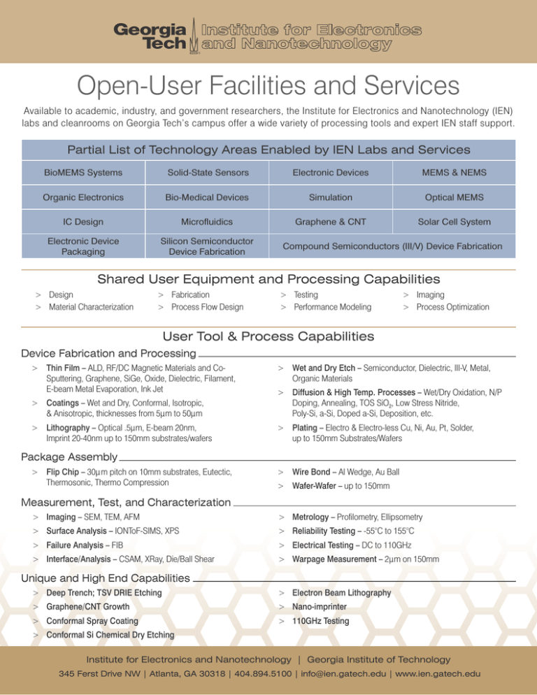
Open-User Facilities and Services Available to academic, industry, and government researchers, the Institute for Electronics and Nanotechnology (IEN) labs and cleanrooms on Georgia Tech’s campus offer a wide variety of processing tools and expert IEN staff support. Partial List of Technology Areas Enabled by IEN Labs and Services BioMEMS Systems Solid-State Sensors Electronic Devices MEMS & NEMS Organic Electronics Bio-Medical Devices Simulation Optical MEMS IC Design Microfluidics Graphene & CNT Solar Cell System Electronic Device Packaging Silicon Semiconductor Device Fabrication Compound Semiconductors (III/V) Device Fabrication Shared User Equipment and Processing Capabilities >> Design >> Material Characterization >> Fabrication >> Process Flow Design >> Testing >> Performance Modeling >> Imaging >> Process Optimization User Tool & Process Capabilities Device Fabrication and Processing >> Thin Film – ALD, RF/DC Magnetic Materials and CoSputtering, Graphene, SiGe, Oxide, Dielectric, Filament, E-beam Metal Evaporation, Ink Jet >> Wet and Dry Etch – Semiconductor, Dielectric, III-V, Metal, Organic Materials >> Coatings – Wet and Dry, Conformal, Isotropic, & Anisotropic, thicknesses from 5 µm to 50 µm >> Diffusion & High Temp. Processes – Wet/Dry Oxidation, N/P Doping, Annealing, TOS SiO2, Low Stress Nitride, Poly-Si, a-Si, Doped a-Si, Deposition, etc. >> Lithography – Optical .5 µm, E-beam 20nm, Imprint 20-40nm up to 150mm substrates/wafers >> Plating – Electro & Electro-less Cu, Ni, Au, Pt, Solder, up to 150mm Substrates/Wafers Package Assembly >> Flip Chip – 30 µ m pitch on 10mm substrates, Eutectic, Thermosonic, Thermo Compression >> Wire Bond – Al Wedge, Au Ball >> Wafer-Wafer – up to 150mm Measurement, Test, and Characterization >> Imaging – SEM, TEM, AFM >> Metrology – Profilometry, Ellipsometry >> Surface Analysis – IONToF-SIMS, XPS >> Reliability Testing – -55°C to 155°C >> Failure Analysis – FIB >> Electrical Testing – DC to 110GHz >> Interface/Analysis – CSAM, XRay, Die/Ball Shear >> Warpage Measurement – 2 µm on 150mm Unique and High End Capabilities >> Deep Trench; TSV DRIE Etching >> Electron Beam Lithography >> Graphene/CNT Growth >> Nano-imprinter >> Conformal Spray Coating >> 110GHz Testing >> Conformal Si Chemical Dry Etching Institute for Electronics and Nanotechnology | Georgia Institute of Technology 345 Ferst Drive NW | Atlanta, GA 30318 | 404.894.5100 | info@ien.gatech.edu | www.ien.gatech.edu Georgia Tech Institute for Electronics and Nanotechnology Materials Processed >> Dielectrics: SiO2, Si3N4,SiC, HfO2, ZnO, >> Semiconductor: Silicon/polysilicon ZrO2, AlN, TiN, TiO2, Al2O3, additional dielectrics on request >> Metals: Al, Cr, Ti, W, Ni, Mo, Pt, Fe, Cu, Ir, Pd, >> Nanostructures: SW-CNT, MW-CNT, (Bosch process), Silicon/polysilicon (Cl2based RIE, SF6/O2 RIE, Cl2-based ICP) Silicon/ polysilicon (cryogenic ICP), ITO Graphene, MoS2, SiGe Nanowires Ag, additional metals by request Typical Processing Capabilities >> Dry Etching: Semiconductor: Silicon/ Polysilicon (Bosch process), Silicon/Polysilicon (cryogenic ICP), Silicon/Polysilicon (Cl2-based RIE, SF6/O2 RIE, Cl2-based ICP), ITO; Dielectric: SiO2 (quartz, fused silica), Si3N4 (CxFy-based ICP); III-V: Cl2, BCl3, SiCl4 RIE & ICP; CH4, H2 RIE; HBr-based ICP; Metals – Al, Cr, Ti, W, Ag >> Wet Etching: SiO2, Si3N4 Metals, Organic materials, Others upon request >> High Temperature Processes: Oxidation (wet & dry), Annealing, Polymer curing, Diffusion (solid-source), Drive-in, Sintering >> Thin Films Deposition: RF/DC Sputtering, Evaporation, ALD, PECVD, CVD, LPCVD >> Polymer Deposition: Parylene, Spincoating, Spray-coating >> Lithography: UV Photo, Deep UV (248nm) Photo, Nanoimprint, Electron beam, Surface modification, UV laser-based, Inkjet printing >> Plating: Electro-plating – Cu, Ni, Au, Pt, PbSn Electroless – Ni, Au >> Characterization: Microscopy: SEM/EDX, TEM, FIB-SEM, ToF-SIMS, XPS/ ESCA, UPS, XRD/XRR; Optical - Ellipsometry Reflectometry, FTIR, UV-Vis photospectrometry, Non-contact 3D profilometry, Thin film thickness, Particle sizing (DLS), Particle zeta potential, Contact angle measurement; Other – Surface Plasmon Resonance, Quartz Crystal Microbalance with Dissipation, Thin-film stress mapping, Elastic modulus (Nano-indentation), Atomic force microscopy >> Packaging: Wire bonding, Wafer bonding: Anodic Bonding/Glass Bonding, Chemical Mechanical Polishing, Flip-chip bonding Lapping, Lamination, Thermal Compressive Bonding Key Equipment >> High Temperature Furnaces: Tystar; oxidation, solid-source dopant, and anneal furnaces; Lindberg oxidation, anneal, sintering furnaces; Tystar mini-oxidation & diffusion, MRL oxidation & anneal >> Etching: RIE – Unaxis, Vision, Oxford, Oxide, Plasma-therm, Plasma-therm SLR; Deep RIE – STS HRM, Oxford Cryogenic ICP, Trion ICP, Plasma-therm ICP, STS AOE ICP, STS Multiplex ASE ICP, STS Pegasus ICP, STS SOE ICP; Plasma Etcher – Gasonics Asher, Yes Plasma Cleaner, Chemical Dry – Xactix XeF2: Other – AMMT HF Vapor; Stripper: Samco UV Ozone >> Physical Vapor Deposition: Sputtering – Denton Discovery RF/DC, Denton Discovery II, Kurt Lesker PVD-75 RF, Unifilm, CVC DC; Evaporation – CHA Metal, CHA Dielectric, Denton Explorer I Metal, Denton Infinity Metal, PVD75 Filament, CVC E-beam >> Polymer Deposition: Spin/Spray Coat – Suss Altaspray, RC-8 track coater, RC-8; BLE, SCS G3P8, EVG 101, Laurel, CEE; Passivation: SCS Parylene Coater >> Rapid Thermal Processing: Jetfirst, SSI, AET >> Lithography: Optical Mask Align – Suss: TSA MA-6, MA-6, MA-6/BA-6us, EVG 620, OAI, E-beam – JEOL JBX, Laser Writer – Microtech LW405, Nano-Imprint – Jetlab inkjet, Obducat, Bioforce Nanoenabler >> Chemical Vapor Deposition: PECVD – Oxford ICP, Black Magic CNT, Surrey CNT PECVD, FirstNano Graphene Furnace, FirstNano SiGe Nanowire Furnace, FirstNano Sulfurization Furnace, FirstNano CNT system, Plasma-therm, STS, Unaxis; LPCVD – Tystar TEOS, Tystar silicon nitride, Tystar doped polysilicon (N&P); ALD – Cambridge Fiji >> Characterization: Profilometers – Dektak 150, Tencor P15, Veeco Dimension 3100 AFM, Wyko NT3300 Optical; Electron Microscopy – SEM – Zeiss Ultra 60, Hitachi 8230, Hitachi 4700, LEO 1530, Hitachi 3500, Hitachi 3700 VP; TEM – Hitachi 7700 TEM; Ellipsometry – Woollam M-2000 VI, Woollam VASE; Nanospec Reflectometer; Optical Microscopy – Olympus LEXT OLS-4000 laser confocal, Olympus IR, Keyence Digital; Spectroscopy – Fisher UVVis, GE SPR, Thermo Almega Raman, DAGE XD7600NT X-ray tomography; Surface Analysis – Kratos Axis Ultra XPS, Thermo K-Alpha XPS, IonTOF 5 ToF-SIMS; Focused Ion Beam – FEI Nova Nanolab 200 FIB/SEM; Cyrstallopgraphy – Panalytical MRD XRD, Other Techniques – Malvern Zetasizer, SCA-2500 surface charge analyzer, FSM 900TC-VAC, Qsense QCM, Rame-Hart 250 Contact Angle, Hysitron Triboindenter, Dage Die Shear >> Packaging: Wafer/Chip Bonding – Karl Suss SB-6, SB-8e Logitech SS, Finetech Lambda; Wire/Ball Bonding – K&S 4523 Semiautomatic, K&S 4523 Wedge, K&S 4522, K&S 1472; BGA rework station Institute for Electronics and Nanotechnology | Georgia Institute of Technology 345 Ferst Drive NW | Atlanta, GA 30318 | 404.894.5100 | info@ien.gatech.edu | www.ien.gatech.edu

