Downlaod1
advertisement

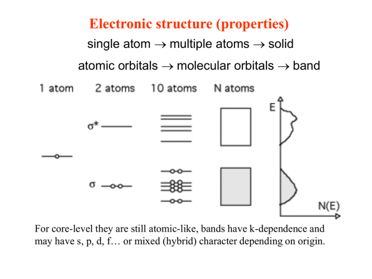
Electronic structure (properties) single atom multiple atoms solid atomic orbitals molecular orbitals band For core-level they are still atomic-like, bands have k-dependence and may have s, p, d, f… or mixed (hybrid) character depending on origin. Bands Bands may be separated by band-gaps of energy Eg. Depending upon number of electrons and DOS, band may be filled, partially filled or empty. Top (partially-)filled band called valence band. Bottom empty band called conduction band. Work function Ev Energy require to move electron from EF to EV at the surface called Workfunction (for semiconductors and insulators from the most loosely bound electrons inside the solid). Normally in the order of electron volts. Work function Work function affects thermionic emission, the contact potential between two solids, filed emission, and the bonding of absorbate atoms to a surface. Work function mainly depends on the depth W of the attractive potential for the conduction electrons inside the solid (bulk property). Surface contributions to W (work function f): Image potential Surface double layer (surface contamination, crystallographic surface orientation). The attractive force for –e outside the metal: e2/4pe0(2d)2 Surface double layer The surface atoms unbalanced distortion of the electron clouds increased electron density between the cores compared with the bulk A double layer with either net positive or net negative charge at the outside. Electric double layer Influence on work function in the order of a few tenth of electronvolt. Distortion of charge at the surface Charge distribution near the surface Charge distribution near surface of a Jellium model. Orientation of surface Density of atoms Charge density work function Experimental results Methods for measurement? Step density effects Monolayer Xe absorption effect Electronic surface states The electronic states exists only at surface Semi-Infinite Chain in the Nearly-Free Electron Model for Surface States In this model in the bulk there is potential with cosine function: V(z) = 2 Vb cos (2pz/a) There is equation to solve: (-h2/2m d2/dz2 + V(z)) f(z) = E f(z) For the bulk we have solution like in the Fig. b Semi-Infinite Chain in the Nearly-Free Electron Model for Surface States With real wave vector k: the matching (both f and df/dz) of the wave function inside the solids and the exponentially decaying electron wave function at the vacuum side gives one solution for the surface, eg. Bloch waves inside the solid with exponentially decaying tails on the vacuum side. With complex wave vector k: we have waves on both side exponentially decay. The matching of both side allows only one energy values for a wave vector, this energy is in the forbidden bulk energy gap. The solution with imaginary k have energy eigenvalues falls inside the energy gap! Surface States of a 3D crystal In 3d each k will give its own E(k||), therefore we have “bands” (with different k together). However, for surface state, there is no k dependence, there is only single line. In-plane is still bloch waves!! The surface states can propagate with bulk states can mix with them, these surface states therefore propagate deep into bulk with large amplitude at the surface: surface resonance. Electronic states: 1D 2D 3D K|| k One an atom have only a state in the Brillouin zone, with increasing number of atoms in 1D case, there will be one band level. For the surface with increasing atom layers K|| experience single band level to bands and K from 1 state to one band level. Intrinsic Surface states Exists on clean and well-ordered surface and have 2D translational symmetry parallel the surface. Those can be described by nearly-free electron model are called Shockley States. they have complex wave vectors with amplitude exponentially decaying into the solid. Those can be described by tight-bonding approximation are called Tamm states. These are due to missing bonding partners and have less overlap of wave function. The splitting and shift of the energy levels is smaller than in the bulk. Basically every orbital involved in chemical bonding gives one surface state level. Higher-lying state conduction-band like and therefore acceptor-type. In reality, Intrinsic Surface states states can Lower-lying state valence-band like and therefore donor-type. For be built conduction band type surface states, the charge character: of both Neutral (empty) negative (with electron) type of For valence band type surface states, the charge character: bands. Positive (empty) neutral (with electron) In the extreme case, the bonds are broken and the remaining lobes of the orbital stick out from the surface called dangling bonds, the surface states then called dangling-bonds states. If the surface-induced modification of the chemical bonds are among the topmost several layers, these surface states are back bond states. Extrinsic Surface states The surface states due to the defects (missing atoms, line defects) or adsorbed atoms have no 2D translational symmetry parallel the surface. They are localized where the defects or adsorbed atoms exist and the bonding geometry for the surrounding atoms changed. Surface States for metal 1. s-/p-like states Simple metal Al, Na, Mg, etc have bulk bands derived from sp- electrons, which are free electron like. The nearly free electron model for surface states is suitable for such systems. These surface states lies in the gap of bulk bands and have also parabolic dispersion. Surface States for metal 2. d-like states Transition metal have d bands, which are very localized and therefore with much less dispersion than sp band. The d bands cross and hybridize with sp bands and lead to new gaps where the surface state can exist. They lies closely to the high lying bulk states and have also different dispersion (not parabolic). Layer-resolved Local Density of States (LDOS) d electrons localized + Surface atoms with fewer neighbours (more free atom like) different surface layer DOS (sharper) Surface core-level shift In order to keep the charge neutrality (the same Fermi energy level), for those with d bands less than half filled (< 5), the core level have negative shift (higher binding energy) and for those more than half filled have positive shift. Image-potential Surface States There are surely unoccupied (empty) surface states above the Fermi energy, among them there are Image-potential Surface States, which are due to the approaching electron captured by the image potential which can falls into the bulk bands gap and behave similar like bulk-band derived surface states. Image-potential Surface States The energy of the trapped electron have a eigen value of such states en, therefore the total energy of the image-potential surface states: E(k||) = h2k||2/2m* -en + ef These states therefore have parabolic dispersion and less sensitive to contamination. They are with fixed energy to vacuum level (change kinetic energy as f change). For bulk band derived surface states: a. sensitive to contamination. b. within gap of the bulk bands. c. dispersion only on k|| Also for Image-potential ones Surface states on semiconductor Each dangling bond orbital will result in a surface state for nonreconstructed surface, however, most semiconductor do have reconstruction and makes situation complicated!!! Surface states on semiconductor Reconstruction on the surface is intimately connected with the dispersion of surface states. The study of the surface states, on the other hand, can help to construct and verify surface structure models.


